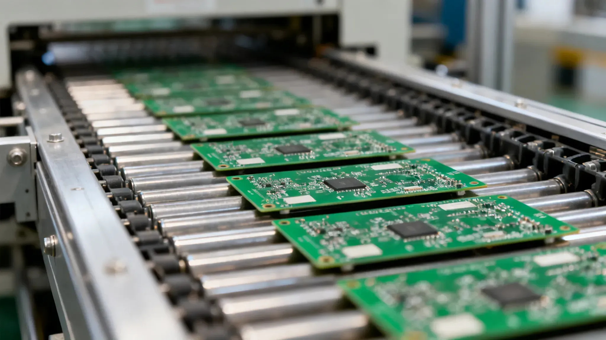

Silk-Screen Verification Checklist for PCBA RFQs
Buyer-side specification, inspection, and RFQ checks on this technical topic. Not a hobby explainer. Request a quote on IC-Online.
IC-ONLINE channel: Identify PCBA Silk-screen printing(part2)#pcb #pcba #smt #chip #capacitors.
When Silkscreen Details Derail PCBA Quotes
A fully assembled PCB arrives, boards are loaded into the test fixture, and the technician can’t orient the regulator: the pin‑1 dot is missing, smeared, or hidden under a via tent. The board spins, the wrong IC gets placed, and a $15,000 rework bill hits before the first article passes. That kind of failure — silent until assembly — is exactly what a poorly specified silkscreen legend invites into a PCBA program.
Silkscreen verification isn’t an artwork afterthought. It’s the visual language that operators, field service engineers, and automated optical inspection (AOI) systems use to confirm component position, polarity, and board revision. When the legend is illegible, ambiguous, or simply absent from the RFQ dataset, you inherit risk across the entire supply chain: PCB fabrication, SMT placement, inline inspection, and end‑of‑line repair. Buyers see the fallout as component scrap, misplaced BGA packages, and even latent field failures where a reversed electrolytic capacitor isn’t caught because the polarity bar faded during wave soldering.
One common scenario: a design team generated silkscreen Gerbers with 0.12 mm line widths, but the chosen fabricator’s standard screen‑printing process can only hold 0.18 mm. The RFQ didn’t call out the requirement, the shop printed what their tooling allowed, and the resulting legend smeared across fine‑pitch pads. Another all‑too‑real story: a contract manufacturer substituted black silkscreen on a dark ENIG substrate, assuming the contrast was fine, only to discover that the AOI camera couldn’t distinguish reference designators from the background — forcing manual inspection for a 10,000‑unit build. Both of these are avoidable, and both trace back to a single document: the RFQ.
To ground the conversation, watch this short PCBA silk‑screen printing overview video from IC‑ONLINE. It demonstrates how a properly registered silkscreen layer looks after printing and reflow, and it’s a quick reality check for anyone writing manufacturing notes. The visuals are worth 1,000 words when you’re trying to explain why “just print white” doesn’t work on every surface.
Silk-Screen Process Essentials: Parameters You Can’t Afford to Ignore
At its heart, PCB silkscreening is a transfer of ink through a mesh screen onto the board surface, cured to bond permanently. The dominant inks are epoxy‑based and UV‑curable formulations, each with distinct adhesion profiles, chemical resistance, and opacity. Epoxy inks deliver excellent adhesion to FR‑4 and solder mask, while UV‑curable systems are favored in high‑speed lines because they cure instantly and produce crisp edges at finer resolutions. The choice isn’t just aesthetic; it directly affects the price you pay in an RFQ because it determines process cycle time, yield at tight geometries, and compatibility with surface finishes like ENIG, immersion silver, or OSP.
When a buyer or engineer fills out a PCBA RFQ, four parameters drive the conversation with the fabrication team. Define them clearly upfront, and you’ll avoid requotes, design‑for‑manufacturability (DFM) pushbacks, and cost surprises.
- Minimum line width and character height. What’s the smallest legend element on your board — a polarity triangle, a tiny reference designator between 0201 pads, or a board revision string? The fabricator needs to know if they can achieve it with the nominated process.
- Ink color and contrast against the solder mask. White is standard, but yellow, black, and even red may be required for brand identity or optical inspection. On dark substrates or low‑contrast finishes, you must verify readability with the specific ink‑mask combination.
- Legend‑to‑pad clearance. Ink on a pad risks solderability defects and can mask tombstoning indicators. The IPC-4781 qualification is often invoked here; the RFQ should state a minimum clearance value, typically ≥0.15 mm for screen‑printed legend.
- Adhesion and peel strength. You need the legend to survive wave soldering, cleaning, and rework cycles. Peel strength (cross‑hatch tape test per ASTM D3359 or IPC‑TM‑650) is the measurable proxy for field durability.
Below is a practical reference table that captures the quantitative ranges you’ll see across typical PCB fabrication lines. Note that these are achievable benchmarks; the actual capability depends on the fabricator’s equipment and quality system. Use this table to set your RFQ expectations, and always confirm the specific capability statement from the supplier.
| Parameter | Typical Range (Screen Printing) | Enhanced Capability (Inkjet / LDI) | Impact on RFQ Cost & Quality |
|---|---|---|---|
| Minimum line width | 0.15–0.18 mm | 0.08–0.10 mm | Below 0.15 mm often triggers a process upgrade; confirm with the fabricator |
| Minimum character height | 0.8–1.0 mm | 0.5–0.6 mm | Smaller text may be illegible after solder; use the fabricator’s DFM report to verify |
| Legend‑to‑pad clearance | ≥0.15 mm | ≥0.10 mm | Insufficient clearance leads to ink on pads, blocked AOI, and tombstoning |
| Standard color options | White, yellow, black | White, yellow, black, red, blue | Non‑standard colors may need a color sample approval before production |
| Ink thickness (cured) | 15–35 µm | 10–25 µm | Thicker ink can obscure fine details; thinner ink may lack opacity on dark masks |
| Peel strength (cross‑hatch tape test) | ≥4B (ASTM D3359) | ≥4B | Specify 5B for Class 3 or harsh-environment assemblies |
| Typical registration tolerance | ±0.15 mm | ±0.075 mm | Tighter tolerance required when legend sits near small SMD pads |
| Maximum board size (legend area) | Process‑dependent, often 600×600 mm | Similar, but may have edge‑clearance limits | Check panel‑level artwork requirements for large arrays |
Every parameter in this table connects to an RFQ line item. If you leave “minimum character height” undefined, the fabricator will default to their standard — which might turn your 0.6 mm reference designators into unreadable blobs. When you submit an RFQ, providing explicit values buys you a quote that reflects your actual board, not a generic build that needs later re‑negotiation. Moreover, peel strength and ink thickness tie directly to the IPC acceptance class you’ll apply: Class 3 boards demand near‑perfect legend integrity because failures in medical or aerospace gear aren’t repairable in the field.
Screen Printing vs. Inkjet vs. LDI: Which Legend Method Suits Your RFQ?
The method you choose for creating the legend defines minimum line width, turnaround speed, color flexibility, and the per‑board cost structure. Traditional screen printing remains the volume workhorse — low material cost, high throughput, but it requires a physical stencil for each artwork and struggles below 0.15 mm features. Digital inkjet legend printers, which jet UV‑curable ink directly onto the board, eliminate the stencil and deliver comparable resolution with greater color agility. For the highest density designs, laser direct imaging (LDI) can image the legend onto a photo‑sensitive ink layer, achieving line definitions approaching 0.05 mm.
Each process carries a different setup‑cost and unit‑cost curve, and your RFQ must align the technology to the production volume and design density. A 50‑piece prototype run with fine‑pitch components might justify inkjet or LDI to avoid a costly screen, while a 100,000‑unit consumer board is almost certainly best served by a traditional screen printing workflow. The table below breaks down the core trade‑offs that your RFQ should address.
| Comparison Metric | Traditional Screen Printing | Digital Inkjet Legend | Laser Direct Imaging (LDI) | Selection Guideline |
|---|---|---|---|---|
| Minimum line width | 0.15–0.18 mm | 0.10–0.12 mm | 0.05–0.08 mm | Choose inkjet/LDI when legend elements fall below 0.15 mm |
| Resolution / edge sharpness | Good, slight bleeding possible | Very good, clean edges | Excellent, photolithographic quality | For high-density BGAs and QFNs, LDI provides the most precise pin‑1 marks |
| Ink thickness and durability | 15–35 µm, robust with epoxy | 10–20 µm, UV-curable | 5–15 µm, photo‑imageable | Thicker epoxy suits rework‑intensive environments; LDI is thinner but still meets Class 2 adhesion |
| Setup cost / tooling | Screens required (~$50–150 per color) | No physical screen; only digital setup | No screen; requires photo‑tool if not fully digital | For prototypes ≤ 200 boards, inkjet or LDI avoids screen charges |
| Unit cost at volume | Lowest at high volume | Moderate, competitive above 1,000 units | Higher, typically reserved for complex low‑ to mid‑volume | Use inkjet as a bridge from NPI to mass production to avoid re‑qualification of legend quality |
| Color capability | Typically white, yellow, black; others on request | Wide gamut; white, yellow, black, red, blue, green | Limited to colors of the photo‑imageable ink system; often white only | If your RFQ calls for non‑white on OSP or immersion silver, inkjet offers the fastest color changeover |
| Panel size / format flexibility | Limited by screen frame size | Flexible; most printers handle up to 24"×30" | Similar to panelization in standard LDI equipment | For large arrays with step‑and‑repeat, confirm the fabricator’s maximum image area |
After you’ve settled on a method, the inspection criteria remain the same. Whether the legend comes from a screen, inkjet, or LDI, IPC‑A‑600 defines the acceptance levels for defects like bridging, smearing, missing characters, and adhesion loss. You can review the visual criteria at IPC’s A‑600 standard page and incorporate the target class into your RFQ notes. If you don’t cite a class, most fabricators default to Class 2, which allows some legend imperfections that might not be acceptable for a high‑reliability power supply or avionics board. Specifying the right legend method plus the correct IPC class in your RFQ is the difference between a board that passes first article and one that triggers a corrective action report.
The RFQ Verification Checklist: 10 Silkscreen Details to Confirm Before Placing an Order
At this stage, you have a complete set of silkscreen Gerbers and a fabrication drawing. You’ve selected a legend process. Now the RFQ must be airtight. Missing even one detail can push your board into a gray zone where the supplier makes assumptions that conflict with your design intent. The following checklist — distilled from dozens of PCBA RFQs — covers the ten highest‑impact items. Verify each one before you hit send. For an extra safety net, use the checklist as a supplier‑side response template: require the fabricator to confirm each point in their quotation.
| No. | Detail to Verify | Verification Action | Risk if Ignored |
|---|---|---|---|
| 1 | Silkscreen Gerber files are present and named correctly | Open the dataset in a Gerber viewer; confirm top (GTO) and bottom (GBO) layers. Note layer names in the RFQ. | Fabricator may omit the legend entirely, leaving bare boards with no markings for assembly. |
| 2 | Pin‑1 indicators, polarity marks for diodes and capacitors match the footprint library | Overlay the silkscreen layer with the paste mask and component placement; verify that every polarized device has a visible dot, chamfer, or “+” mark. | Reversed electrolytics, misplaced BGAs; $100+ in rework and potential field failures. |
| 3 | Reference designators are legible at target character height and line width | Measure a sample designator in the Gerber; ensure it’s ≥0.8 mm tall for screen printing or ≥0.5 mm for inkjet. | Illegible text forces manual assembly aids, slowing placement and increasing labor cost. |
| 4 | No legend ink on pads or within minimum clearance zone | Run a DRC check with pad‑to‑legend clearance ≥0.15 mm (screen) or ≥0.10 mm (inkjet/LDI). | Ink on pads compromises solderability and masks tombstoning; AOI rejects pile up. |
| 5 | Legend color and contrast specified for each surface finish | State “White legend on green mask, ENIG finish” or similar. Request a color swatch if using yellow or black. | Low‑contrast combinations (e.g., black legend on dark blue mask) render AOI and manual inspection unreliable. |
| 6 | Panel fiducials and board‑level fiducials are free of legend encroachment | Check that all fiducial clear areas are at least 2× the fiducial diameter and have no ink crossing the zone. | Fiducial recognition fails, stencil alignment drifts, and placement accuracy degrades. |
| 7 | Panel border markings (tooling holes, score lines, tab routes) are clearly defined and not confused with legend graphics | Assign a separate mechanical layer for panel features; ensure silkscreen doesn’t print over breakaway tabs. | Operator cuts along a silk‑screen line meant for panelization, destroying boards. |
| 8 | IPC acceptance class for legend defects is cited (Class 2 or 3) | Add a note: “Legend shall meet IPC‑A‑600 Class [2/3] acceptance criteria.” | Without a class, the fabricator may ship boards with bridging, missing characters, or peeling legend that you consider rejectable. |
| 9 | First‑article images or 1:1 print approval process is defined | Request a digital photo of the legend on the first article prior to assembly; specify in the RFQ. | Errors caught only after assembly require full board scrap and re‑fabrication. |
| 10 | Critical component markings that must match the silkscreen are cross‑checked with the BOM | Use IC‑ONLINE to verify that the purchased parts’ package markings align with the silkscreen reference designators and orientation marks before assembly. | A mismatched package body mark can confuse the operator, causing a mirrored placement that escapes test. |
When you work through this checklist, you’re not just verifying artwork; you’re building a contractual clarity layer around your PCBA RFQ. Many of the most frustrating silkscreen disputes — “the text is too small,” “the color bled,” “the pin‑1 dot is missing” — vanish when the drawing, Gerbers, and RFQ notes all speak the same language. And whenever a component’s orientation depends on a tiny laser‑etched mark, a quick cross‑check on IC‑ONLINE against the device datasheet can confirm that the silkscreen callout and the physical part are consistent.
Silkscreen RFQs: Questions Engineers and Buyers Should Ask
Q: How do I confirm the manufacturer will use the right silkscreen color, especially on ENIG or OSP finishes?
Specify the desired color (white, yellow, black, etc.) directly in the RFQ notes and link it to the surface finish: “White epoxy silkscreen on ENIG (immersion gold) finish, Class 2.” Request a color sample or a high‑resolution photograph of a similar board from the fabricator’s portfolio. If your application demands a specific contrast ratio — say, for AOI — ask for a ΔE (color difference) target. On OSP finishes, white ink can occasionally show a slight yellow shift after reflow; confirm with the supplier that the chosen ink formulation is qualified for your reflow profile.
Q: What is the acceptable minimum line width for silk‑screen legend on a dense HDI board?
For traditional screen printing, the practical floor is 0.15 mm; below that, you risk smearing and bridging. On HDI designs with 0.4 mm pitch BGAs and tight routing, that’s often insufficient. Inkjet legend can reliably produce 0.10 mm lines, and LDI can push below 0.08 mm. The RFQ must state the required minimum line width and ask the fabricator to confirm capability for your layer count and board thickness. Don’t assume — have the supplier’s DFM engineer sign off; otherwise, you’ll get boards with beautiful traces and illegible orientation dots.
Q: Does the silkscreen layer need a separate Gerber file, and how do I prevent it from being omitted?
Yes, always provide a dedicated silkscreen Gerber file for the top and bottom sides (typically GTO and GBO). Some EDA tools combine legend into a composite print layer; break it out before generating manufacturing outputs. Add a bold RFQ note: “Missing silkscreen Gerber files will be flagged before quotation — do not proceed without them.” Before submission, open the full Gerber set in a viewer such as Gerbv or ViewMate and confirm that the silkscreen layer appears correctly. This five‑minute check catches name mismatches, swapped layers, and omitted file attachments.
Q: Can I request non‑white silkscreen on a board with immersion silver or lead‑free HASL?
Yes, but verify adhesion and opacity directly with the fabricator. Some black inks can appear translucent on bright silver finishes, reducing contrast. Lead‑free HASL surfaces are more tolerant, but the slightly irregular topography may affect edge sharpness. Specify the ink type (epoxy, UV‑curable) and ask for a process compatibility statement in the quotation. If possible, request a test coupon or a photograph of a panel that used the same ink‑finish combination. Without upfront verification, you risk receiving boards where the legend flakes off after a single rework cycle.
Q: How do I verify polarity markers and pin‑1 indicators for BGA and QFN packages before finalizing the RFQ?
Overlay the silkscreen layer with the component footprint and the paste mask in your EDA tool. For BGA packages, the pin‑1 indicator should be a clear dot or chamfer that is not hidden by the corner pad or a nearby via. For QFNs, the exposed pad and the pin‑1 mark must be unambiguously placed — a small silk‑screen triangle or text “1” that sits outside the body outline is easiest for operators. After visual verification, request a 1:1 scale print from the fabricator or a first‑article photo that shows the legend alignment against a dummy component. Dense boards with 0.4 mm pitch devices are unforgiving; a 0.2 mm misregistration can obscure the mark entirely.
Q: Which IPC inspection class applies to silkscreen defects, and should I cite it in the RFQ?
IPC‑A‑600 defines three classes: Class 1 (general electronic, cosmetic flaws acceptable), Class 2 (dedicated service, some legend imperfections allowed), and Class 3 (high reliability, legend must remain legible and intact after thermal stress). For industrial controls, consumer IoT, and most commercial products, Class 2 is sufficient. For medical, aerospace, or military assemblies, specify Class 3. You must state the target class in the RFQ; it directly influences the acceptance limits for bridging, smearing, missing characters, and adhesion testing. Without it, the fabricator will default to their internal standard — and you may find yourself arguing over whether a partially missing reference designator is a reject or not. Add a short note: “Legend defects shall be evaluated per IPC‑A‑600, Class 2 (or 3).”
References & Further Reading
- Identify PCBA Silk‑screen printing (IC‑ONLINE video)
- IC‑ONLINE electronic component sourcing platform
- IPC — Association Connecting Electronics Industries
- IPC‑A‑600 Acceptability of Printed Boards
- Sierra Circuits: PCB Silkscreen Guidelines
- Altium: PCB Silkscreen Standards and Guidelines
- Digi‑Key: PCB Silkscreen 101
- ASTM D3359 Standard Test Methods for Rating Adhesion by Tape Test
- IPC‑TM‑650 Test Methods Manual
Every PCBA RFQ that reaches a contract manufacturer carries a set of assumptions. Silkscreen legend — the visible face of the board — should never be left to assumption. By defining line widths, colors, adhesion requirements, and the acceptance standard, you close the gap between what you designed and what the fabricator builds. The result is fewer requotes, faster first‑article approval, and an assembly line that never guesses polarity.
Ready to quote a PCBA build with tight silkscreen requirements? Upload your BOM and fabrication files to IC‑ONLINE and request a comprehensive quotation — mixed BOM, flexible MOQ, and no‑surprise lead‑time confirmation. Your silkscreen artwork deserves the same scrutiny as your signal integrity; we’ll help you bridge the two.