Smart Band & Watch BOM: Wearable SoCs, Sensors, PMIC, and Volume Component Supply
Smart Band & Watch BOM: Wearable SoCs, Sensors, PMIC, and Volume Component Supply
Why 2026 Is Testing Smart Band and Watch Component Supply Chains
Smartwatch shipments clawed back to growth in 2025, with Huawei, Xiaomi, Apple, and Samsung all reporting volume gains, and China’s domestic market providing an extra surge of demand (Digitimes). For engineering and procurement teams, that rebound is a mixed blessing. As 2026 unfolds, the same source warns of tightening cost and feature pressures that will challenge how you build the bill of materials (BOM) for a smart band or watch. You’re no longer just picking components; you’re balancing innovation with lead‑time risk, single‑source exposure, and PCB real estate that’s already squeezed to the limit.
At the centre of this balancing act sit the SoC and PMIC choices that anchor every wearable design. NXP’s smartwatch reference platform and its dedicated application note (AN14891) outline the power‑management architecture that many teams will adopt, while Renesas and Nordic Semiconductor have expanded their own ultra‑low‑power BLE SoC and PMIC portfolios. The common thread is that every component decision now has a direct procurement consequence—whether it’s a 16‑week lead time on a Bluetooth SoC, a single‑sourced PPG sensor module, or a PMIC that fits within a 25.9 mm² footprint. The table below captures the key drivers that are reshaping the wearable component supply chain right now.
| Driver | Mechanism | Procurement Impact |
|---|---|---|
| Rebound in China‑centric smartwatch demand | Strong domestic shipments in 2025 lifted overall volumes, pulling in more components. | Hot‑runner SoCs and PMICs may see allocation; buffer stock through distribution becomes critical. |
| Cost‑feature squeeze in 2026 | OEMs push for richer features (larger displays, more sensors) while still targeting mid‑range price points. | BOM cost targets tighten, forcing buyers to negotiate longer‑term agreements or multi‑source more aggressively. |
| Supplier consolidation around proven PMIC platforms | NXP, Nordic, and Renesas are anchoring reference designs with their own PMIC families. | Second‑source qualification becomes harder; teams must pre‑qualify alternatives early in the design cycle. |
| Miniaturisation and PCB area constraints | Smart bands and watches demand that power management occupy less than 30 mm² total. | PMIC area directly influences design lock‑in; switching to a different vendor may require a full board re‑spin. |
| Evolving sensor accuracy requirements | Optical heart‑rate and high‑precision IMUs are moving from single‑vendor proprietary modules to more open ecosystems. | Multi‑sourcing is possible but still requires careful qualification of optical stacks and calibration firmware. |
Each of these drivers forces you to look at the BOM not as a static list but as a live risk map. The next section breaks down exactly what goes into that map.
What Lives Inside a Smart Band or Watch: The Core BOM Breakdown
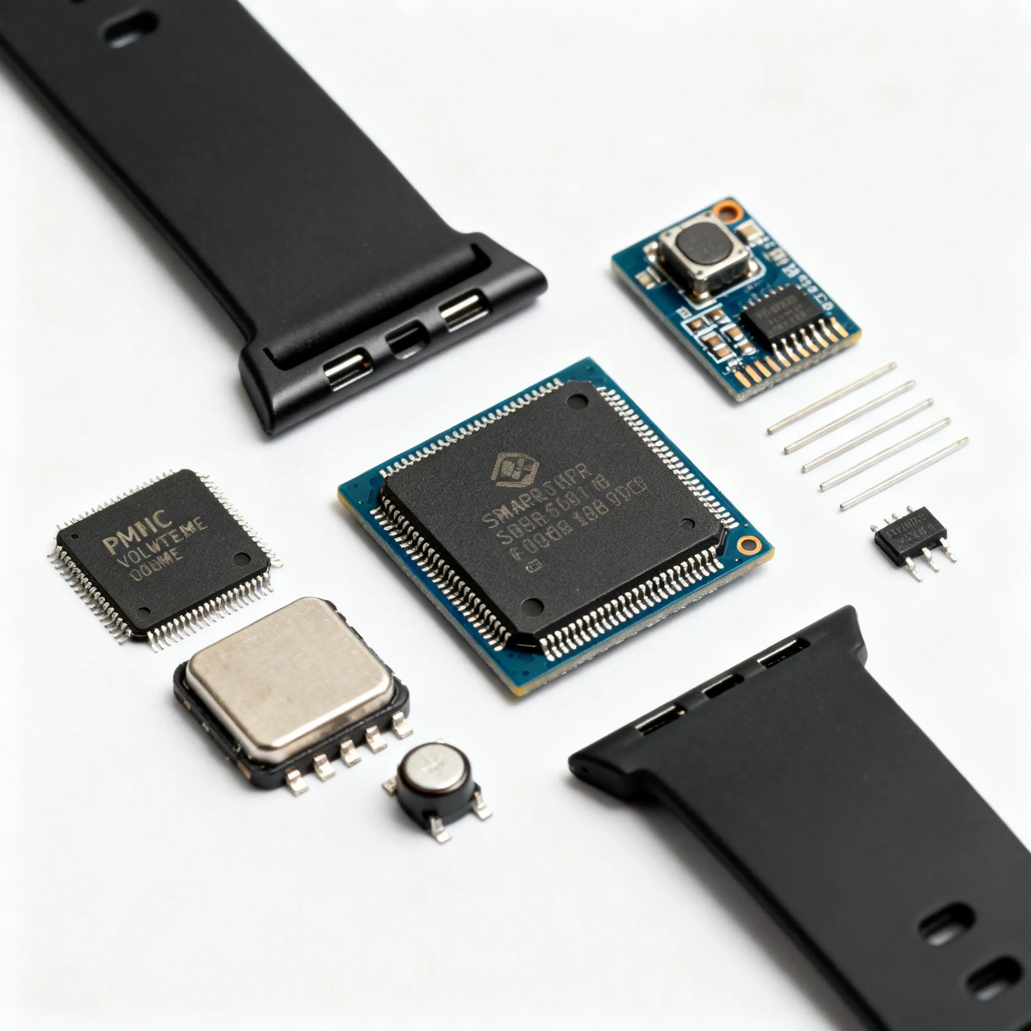
Even the simplest fitness band packs a surprising amount of functionality into a wrist‑sized PCB. The NXP smartwatch block diagram (NXP Smart Watch) and the Renesas wearable solutions portfolio (Renesas) both show a common architecture: an ultra‑low‑power SoC or MCU with integrated BLE, a multi‑rail PMIC handling battery charging and multiple voltage rails, motion and biometric sensors, memory, and a display power path. For a smart band, the SoC may be a single‑chip Bluetooth Low Energy device like the Renesas DA14531 or a Nordic nRF52 series, while a smartwatch often adds a more capable application processor or a richer MCU with external flash.
Power management is the silent hero. The Nordic nPM1304, an evaluation board for which is stocked by Rutronik (Electronics Weekly), integrates a 4‑100 mA linear charger, multiple buck converters, and LDOs. NXP’s PCA series PMICs, detailed in application note AN14891, are purpose‑built for wearable applications and handle the tight sequencing requirements of low‑power MCUs. EDN’s practical guide (EDN) notes that a typical fully integrated PMIC solution for a smart watch occupies roughly 25.9 mm² of PCB area—a benchmark that every design team should keep in mind, even if a smartwatch’s larger board can stretch a little further.
The table below gives you a sourcing‑ready snapshot of the core BOM blocks, representative part families, and the procurement considerations that matter in volume.
| BOM Block | Representative Part Families | Key Parameters | Procurement Notes |
|---|---|---|---|
| Ultra‑low‑power SoC / MCU + BLE | Nordic nRF52840, Renesas DA14531, NXP KW36/36A | Active current <5 mA @ 0 dBm TX, deep‑sleep <2 µA | Lead times 12–16 weeks; buffer via distribution. Multi‑source qualification often requires RF re‑certification. |
| Multi‑rail PMIC | Nordic nPM1304, NXP PCA series, Renesas RAA2S series | Integrated charger, 2‑3 bucks, 2‑4 LDOs; total area ≤ 25.9 mm² | Evaluation boards (e.g., Rutronik‑stocked nPM1304) accelerate prototyping. Pin‑compatible alternatives are rare; plan early. |
| 6‑axis IMU | Bosch BMI270, ST LSM6DSO, TDK ICM‑42688 | Gyro noise ≤ 5 mdps/√Hz, accel noise ≤ 150 µg/√Hz | Generally multi‑sourced with similar footprints; verify register map and FIFO behaviour. |
| Optical heart‑rate (PPG) module | Analog Devices ADPD188, Osram/Silicon Labs Si114x, Maxim MAX861xx | Multi‑channel, integrated LED drivers, typical SNR ≥ 100 dB | Limited vendor pool; qualifying a second module requires optical stack re‑characterisation. Long‑term supply agreements advised. |
| Memory (external Flash / PSRAM) | Winbond, Macronix, ISSI | SPI or QSPI, 8‑64 Mbit, 1.8 V | Mature supply chain with short lead times; watch for EOL on older densities. |
| Display PMIC / backlight driver | TI TPS65132, Diodes Inc. AP5724 | Single‑ or dual‑output boost, 25‑35 mA LED current | Smartwatch AMOLED panels often require a dedicated PMIC; smart bands may use a simple LDO boost. |
The BOM for a smart band typically stays lean: a single BLE SoC, one PMIC, an IMU, and a PPG module, plus a small memory chip and a few passives. As you move to a full smartwatch, that BOM grows substantially—a difference that we’ll examine next.
Smart Band vs. Smartwatch: How BOM Complexity Drives Different Sourcing Strategies
Hands‑on comparisons from Jointcorp (Jointcorp) and Layers (Layers) make it clear that a fitness tracker and a smartwatch are not just different products; they are different BOM philosophies. The fitness band’s sensor‑and‑display BOM relies on a highly integrated SoC, a minimalist PMIC, and a small monochrome or low‑resolution TFT screen. A smartwatch, by contrast, incorporates an application processor or a more powerful MCU with external RAM, larger storage, a higher‑voltage battery charger, a vivid AMOLED display, and often additional sensors such as an ambient light sensor, NFC, and a microphone/speaker combination. The Jointcorp analysis highlights that sensor accuracy and battery life trade‑offs intensify as the feature set grows.
These architectural differences cascade into distinct procurement profiles. The table below maps how each segment’s BOM complexity affects component buyers and engineering leads.
| Segment / Option | Effect on Sourcing | Procurement & Engineering Notes |
|---|---|---|
| Fitness band OEM (high‑volume, cost‑sensitive) | Consolidated BOM; fewer line items, but high unit volumes increase sensitivity to component price and availability. | Focus on securing long‑term pricing for SoC and PMIC. Multi‑source IMU and memory early. Even a 5‑cent price move on a 10‑million‑unit run is material. |
| Smartwatch OEM (mid‑volume, feature‑rich) | Richer BOM adds application processor, larger memory, NFC, haptics, and display backlight—each with its own lead‑time and qualification demands. | PMIC area budget may relax slightly, but the rail count increases. Qualification costs rise with component count; phase‑in second‑source parts in later product revs to contain risk. |
| Distributors stocking PMIC and SoC evaluation kits | Faster prototyping cycles raise demand for evaluation boards and small‑quantity reel availability. | Rutronik’s stocking of the nPM1304 eval board is a good example of enabling quick design starts. Buyers should check distributor inventory of evaluation kits to shorten NPI. |
| EMS / contract manufacturers | Mixed BOMs—one product may need 0201 passives for a band, another requires 0.4 mm‑pitch BGAs for a smartwatch. | Ensure your EMS partner can handle the fine‑pitch assembly and underfill required for advanced SoC and PMIC packages. Multiple BOM variants demand strict change control. |
For procurement leads, the takeaway is straightforward: the more complex the BOM, the more you need to treat supplier selection as a multi‑phase process that starts during architecture definition, not after the schematic is frozen. The next section dives into the practical side of that process.
Sourcing PMICs and SoCs for Volume: Lead Times, Single‑Source Risks, and Design Pitfalls
NXP’s application note AN14891 provides a detailed power management solution for smart watch and band designs, but it also underscores a harsh reality: the PMIC you choose early will likely dictate your power tree, your PCB layout, and your firmware for the life of the product. EDN’s PMIC selection guide reinforces this by showing that a compact integrated PMIC can save you from routing six discrete rails, but at the cost of flexibility. If you later need to add a haptic driver or a higher‑current NFC rail, that integrated PMIC may no longer fit.
Lead times are equally unforgiving. Most suppliers—Nordic, Renesas, NXP—have stabilised at 12–16 weeks for BLE SoCs and PMICs, but high‑volume spikes can push deliveries to 20 weeks or more. The Digitimes report on 2026 challenges suggests that the cost‑feature balancing act will make OEMs rush to lock in supply, potentially extending lead times further. Tying your design to a single‑source PMIC without a fallback plan is a line‑down risk that procurement teams can’t afford to ignore.
Practical steps to mitigate these risks are summarised in the table below.
| Action | When to Use | Trade‑off |
|---|---|---|
| Qualify a second‑source PMIC with a compatible pinout | During architecture phase, before PCB layout is frozen. | Pin‑compatible PMICs are rare; you may need to accept a slightly different package or external component count. Early engineering investment pays off in supply security. |
| Use evaluation boards (e.g., nPM1304 from Rutronik) to accelerate prototyping | Immediately after selecting a PMIC candidate. | Eval boards shorten firmware development but may not reflect your final layout’s thermal and EMI behaviour. Plan for a quick turn PCB spin once the PMIC is integrated. |
| Consolidate glue logic with Renesas GreenPAK™ configurable mixed‑signal ICs | When the BOM accumulates discrete logic, level shifters, or timing generators. | GreenPAK ICs cut part count and board area, but they add a different design tool chain and require NVM programming. The Renesas wearable portfolio includes GreenPAK for exactly this purpose. |
| Negotiate long‑term supply agreements (LTSA) with lead‑time transparency | For PPG modules, high‑end IMUs, and BLE SoCs that are critical and single‑sourced. | LTSAs may require volume commitments; work with your EMS and distribution partners to forecast accurately. The cost of a line shutdown far outweighs the premium of a guaranteed allocation. |
| Adopt a modular BOM approach for smartwatch variants | When you plan to offer multiple SKUs (e.g., with/without NFC, with/without GPS). | Modules add cost and board area but allow you to swap features without redesigning the core PMIC and SoC layout. This approach also simplifies procurement of the common‑core components. |
The 2026 cost‑feature balance flagged by Digitimes means that the cheapest BOM won’t always be the winning one. A design that can be sourced reliably, with a fallback PMIC and a second‑source sensor plan, offers a lower total cost of ownership even if the BOM spreadsheet shows a slightly higher component cost. We’ve seen this play out in the field: teams that spent an extra two weeks qualifying alternative PMICs during the design phase avoided 12‑week line stoppages when their primary supplier went on allocation.
Smart Band & Watch BOM: The Questions Procurement and Engineering Teams Are Asking
Q: What are realistic lead times for ultra‑low‑power BLE SoCs in 2026?
Most suppliers—Nordic, Renesas, NXP—have stabilised at 12–16 weeks for their mainstream BLE SoC families. However, high‑volume spikes from the China demand rebound or a sudden feature push can stretch lead times to 20 weeks or more. Distributor buffer stock and second‑source qualification are the most effective safeguards. If your design can flex between, say, a Nordic nRF52840 and a Renesas DA14531 with minimal firmware changes, you’ve already bought yourself a lot of supply resilience.
Q: How do we choose between a fully integrated PMIC and discrete power rails for a smart band?
Integrated PMICs like the Nordic nPM1304 or the NXP PCA series save board area and simplify design, which is a major advantage when you’re working within the 25.9 mm² benchmark reported by EDN. A discrete approach—using separate LDOs, a charger IC, and a buck converter—gives you more flexibility for custom power sequencing and can be easier to multi‑source, but it eats up PCB space and increases component count. NXP’s application note AN14891 provides a detailed integrated solution for wearables; the choice hinges on your power‑tree complexity and your space budget. If your band design already pushes the limits of a single‑chip PMIC, consider a hybrid approach: integrate the chargers and buck converters, and keep ultra‑low‑noise LDOs discrete for sensitive analog rails.
Q: What sensor types are hardest to multi‑source, and how do we mitigate risk?
Optical heart‑rate (PPG) modules and high‑precision IMUs with integrated sensor fusion are the trickiest. PPG modules from Analog Devices, Osram, and Maxim are often the only game in town for a given optical stack, and switching to a different module requires re‑characterising the entire optical path—LED wavelengths, photodiode placement, and cover‑glass transmission. High‑end IMUs from Bosch, ST, and TDK may be pin‑compatible, but their register maps and built‑in algorithms differ. Mitigation starts with qualifying two or three approved sensor modules during the EVT phase, and then negotiating long‑term supply agreements with clear lead‑time visibility. For the optical stack, lock in the mechanical design early so that you have a known‑good combination of module and lens.
Q: How does the shift from smart band to smartwatch affect BOM cost and sourcing?
The BOM cost can easily double. A smartwatch adds a larger, higher‑resolution display, more RAM and Flash, an application processor or a richer MCU, and a higher‑capacity battery charger, plus often NFC, haptics, a microphone, and a speaker. The sensor suite may also expand to include an ambient light sensor, a barometer, and a dedicated GNSS receiver. Each new line item brings its own qualification burden and lead‑time risk. The comparison in our article highlights that the smartwatch BOM demands deeper supplier qualification, because a single‑sourced component on a more expensive product carries a larger financial penalty if it goes on allocation.
Q: Should we evaluate PMICs based on the 25.9 mm² benchmark mentioned in EDN?
That benchmark is a useful sanity check for highly compact band designs where every square millimetre counts. For a smartwatch, you may afford a slightly larger PMIC area—say 30–35 mm²—but you’ll need additional rails for NFC, haptics, and a higher‑current display backlight. So rather than treating 25.9 mm² as a hard limit, use it as a starting point to evaluate the trade‑off between integration and the number of rails you truly need. If your power tree requires more than what a single integrated PMIC can deliver, a two‑chip PMIC solution or a hybrid approach may be a better fit, even if it pushes the area beyond that benchmark.
Need components or PCBA support for Smart Band / Watch products? IC-Online helps smart-device OEMs with sourcing and board-level supply — see our Smart Device Solutions or contact our team for a BOM review.
References & Further Reading
- Digitimes: Smart wearable demand rises as 2026 poses challenges in costs and features
- NXP Semiconductors: Smart Watch block diagram and wearable solutions
- NXP Application Note AN14891: Power Management Solution for Smart Watch & Band
- Electronics Weekly: Wearables PMIC evaluation board (Nordic nPM1304 stocked by Rutronik)
- Renesas: Wearable Device Solutions – Low Power, High Integration, & Efficient PMIC
- EDN: Find the right PMIC for your wearable systems
- Jointcorp: Smart Ring vs Fitness Tracker vs Smartwatch Ultimate Comparison 2026
- Layers: Smartwatch vs Smart Band – Key Differences & Which to Choose
- Nordic Semiconductor: nPM1304 PMIC
- IC-Online: Mixed BOM and flexible MOQ sourcing for wearable components
Smart band and watch BOM decisions in 2026 are a tightrope between cost, feature integration, and supply chain resilience. The reference platforms and component families we’ve covered—from Nordic’s nPM1304 to NXP’s PCA series and Renesas’s BLE SoCs—give you a solid technical foundation. The real competitive advantage lies in how you manage the procurement side: qualifying second sources early, locking in lead‑time transparency, and using evaluation boards to cut your bring‑up time. For mixed BOMs that span high‑volume passives and single‑source sensors, IC-Online can help you source the full range of components with flexible minimum order quantities, keeping your NPI schedule on track even when the supply chain tightens.