

Step-by-Step Design of a High-Efficiency Dimmable LED Driver Circuit
Expert guide on Step-by-Step Design of a High-Efficiency Dimmable LED Driver Circuit. Technical specs, applications, sourcing tips for engineers and buyers.
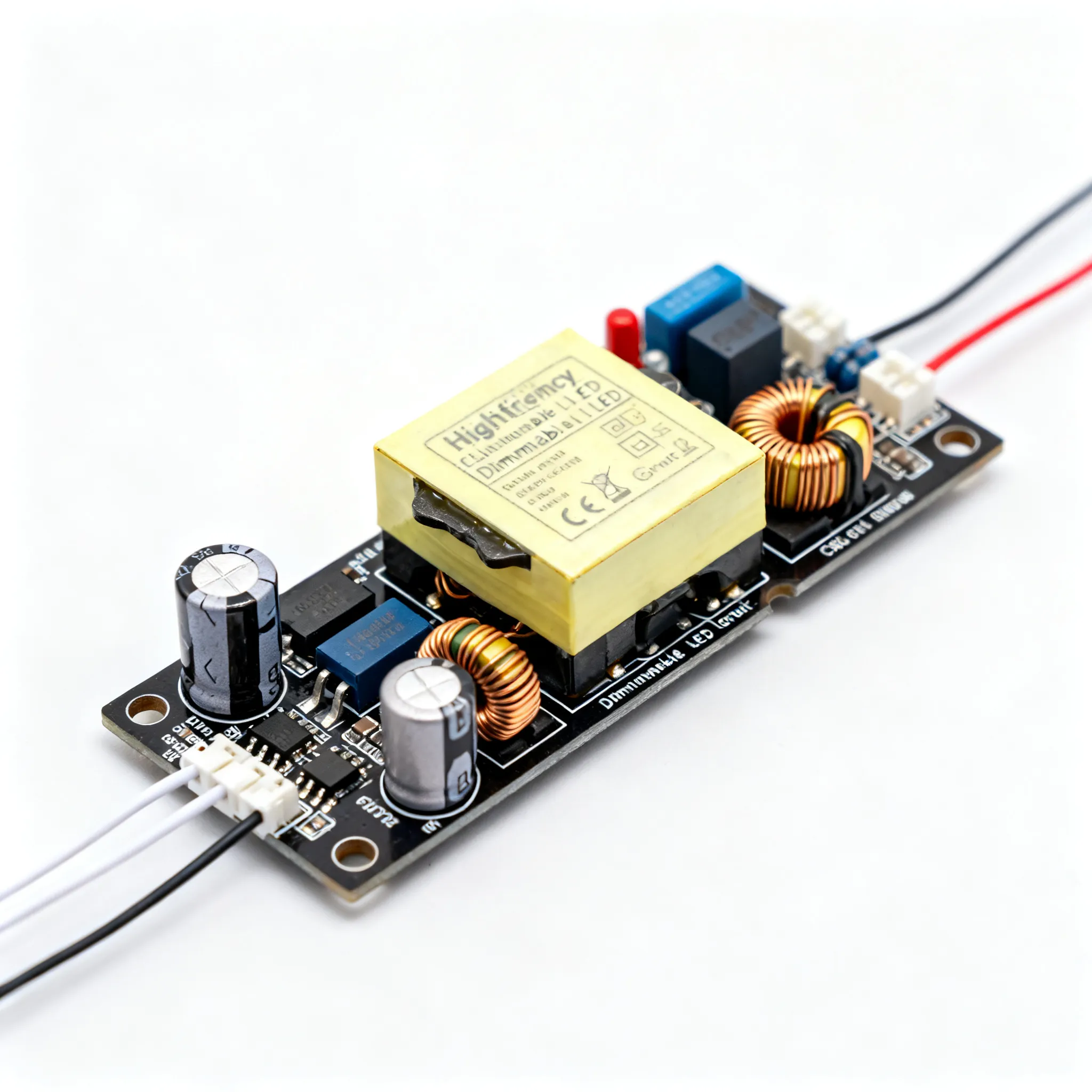
When a Defective Batch Can Trigger a Recall: Why Robust Driver Design Matters More Than Ever
Every production engineer remembers the call they hope never to receive: a field failure rate creeping past the acceptable threshold, luminaires flickering in a hospital corridor, or a dimming circuit that latches at 30% brightness. A PCB manufacturer’s own quality policy, documented at jjled.com, commits to repairing and resending defective batches—and even discussing a full recall “according to real situation.” That admission is not an isolated anecdote; it’s a reflection of how tightly modern LED driver design is coupled to supply chain trust and end-user safety.
As energy regulations tighten—Title 24 in California, EU Ecodesign 2019/2020, and the latest ENERGY STAR® luminaire specification—and as dimming expectations shift from a simple 0–10 V analog signal to flicker‑free, deep‑dimming (<0.1%) performance, a high‑efficiency dimmable LED driver can no longer be treated as a commodity. The driver must anticipate thermal stress from enclosed fixtures, transient load steps when LED strings age, and component tolerances that drift over a 50,000‑hour design life. A single batch of out‑of‑spec flyback transformers or a poorly compensated feedback loop can cascade into thousands of RMA units, erasing the margin from the entire project.
The good news is that with a systematic, step‑by‑step design approach—starting from topology selection, moving through layout and magnetics, and ending with validation of dimming resolution—you can build a driver that hits 93% efficiency, delivers smooth dimming below 5%, and survives the harsh realities of the supply chain. This article walks through each step, using real component data, field‑proven guidelines, and the latest application notes from power semiconductor vendors.
How Constant Current Regulation and Dimming Interfaces Shape Efficiency and Light Quality
At the core of any LED driver is the constant‑current regulator. LEDs are current‑driven devices; their forward voltage varies with temperature and binning, so a constant‑voltage source would cause drastic current swings. Most high‑brightness LED strings require a tightly regulated current—typically 350 mA, 700 mA, or 1050 mA—with a tolerance of ±5% or better to maintain uniform flux and color. The regulator must also respond to the dimming command without introducing perceptible flicker, which the IEEE 1789‑2015 standard quantifies as a modulation depth below 0.5% at frequencies above 90 Hz for low‑risk applications.
A simple dimmable driver circuit, as shown in a Diotec application note, often starts with a linear regulator or a basic buck converter whose current sense resistor is modulated by an external 0–10 V signal. While straightforward, such circuits suffer from poor efficiency when the input‑to‑output voltage differential is large. For higher efficiency, the industry relies on switch‑mode topologies—buck, boost, buck‑boost, or flyback—where the duty cycle is adjusted to maintain a constant average current. AllPCB’s efficiency tips emphasize optimizing the switching frequency, selecting low‑ESR output capacitors, and minimizing the freewheeling diode’s forward drop to reduce power loss. A well‑executed design can push full‑load efficiency above 92%, which directly translates to lower heat sink requirements and a smaller form factor.
The dimming interface is the bridge between the user’s intent and the light output. Three primary methods coexist: 0–10 V analog control, PWM dimming applied to the LED current, and digital protocols such as DALI or DMX. A STMicroelectronics application note (AN2042) illustrates how a VIPower device can perform dimming operations by adjusting the peak current limit, achieving a smooth analog dimming range down to 1%. The choice of interface affects not only the user experience but also the internal control loop: a 0–10 V signal typically feeds a voltage‑controlled current source, while PWM dimming can be applied directly to the enable pin of the regulator IC, risking flicker if the PWM frequency is too low.
Table 1: Typical Performance Parameters for a High‑Efficiency Dimmable LED Driver
| Parameter | Typical Value Range | Units / Notes |
|---|---|---|
| Input voltage (universal) | 90–305 V AC | For global commercial use; 120–277 V AC common |
| Output current | 350–1400 mA | Depends on LED string; ±3% regulation |
| Full‑load efficiency | 88–93% | At 230 V AC, 700 mA output; flyback/buck‑boost |
| Power factor (PF) | >0.90 at full load | Required for commercial lighting >25 W (IEC 61000‑3‑2) |
| Total harmonic distortion (THD) | <20% | Under 15% typical; lower is better for grid‑friendly operation |
| Dimming range (0–10 V) | 10–100% (standard), 1–100% (deep dimming) | IEC 60929 Annex E compliant interfaces achieve 10% minimum |
| Flicker percent (modulation depth) | <1% at 1 kHz PWM | IEEE 1789‑2015 low‑risk region |
| Standby power | <0.5 W | When dimmed to off; ENERGY STAR requirement |
| Case temperature limit | Tc max 85–90 °C | Ensures electrolytic capacitor life exceeds 50,000 h |
| Isolation | 3.75 kV AC (input to output) | Double‑insulated for Class II luminaires |
The table above sets the baseline. Achieving these numbers demands careful attention to the control method. Hysteretic buck converters are simple but suffer from variable frequency operation, which can generate audible noise and make dimming non‑linear. Current‑mode control with a fixed‑frequency PWM controller, such as the popular FL7732 or MP4033, provides better line regulation and a predictable dimming curve. The application note from STMicroelectronics recommends a peak‑current‑mode flyback converter that inherently limits current during dimming, avoiding saturation of the transformer and maintaining efficiency even at low dimming levels. The interaction between the dimming signal and the control loop is critical: if the dimming voltage is simply PWM’d into the feedback pin, the loop may oscillate, causing visible shimmer. The solution is often a hybrid approach—an analog dimming reference that smoothly reduces the current setpoint, combined with a high‑frequency PWM (above 25 kHz) to trim the current when the reference is below 10%.
Buck, Boost, SEPIC, or Linear? Matching Topology to Your Dimming Needs
Selecting the power conversion topology is the first major design decision, and it directly impacts dimming performance, efficiency, and cost. A AllPCB driver selection guide frames the decision around constant current vs. constant voltage architecture, but for dimmable LED strings, the topology must also handle wide input voltage ranges and maintain stability when the load current is reduced to a few milliamps. MicroType’s advanced driver design shows how a simple linear regulator dissipates P = I² × R = 1 W for a 0.5 A current through a 4 Ω resistor, which quickly becomes impractical for multi‑watt LED strings. The WonderfulPCB manufacturing guide underscores that dimmable lights demand high accuracy, like ±2%, for steady brightness—a specification that narrows the topology choices to well‑regulated switch‑mode designs.
Each topology brings a unique set of trade‑offs, and the final choice should be driven by the LED string voltage, the input voltage range, and the required dimming resolution.
Table 2: Topology Comparison for Dimmable LED Drivers
| Comparison Metric | Buck Converter | Boost Converter | SEPIC / Buck‑Boost | Linear Regulator | Selection Criteria & Failure Boundary |
|---|---|---|---|---|---|
| Typical efficiency | 90–95% | 88–92% | 85–90% | Vout/Vin ratio (e.g., 50% at best) | Buck excels when V_in > V_LED; linear is only viable for low‑power, non‑dimmable indicators |
| Dimming performance (analog) | Excellent down to 1% with dedicated IC | Good, but loop compensation at light load is tricky | Very good; symmetrical behaviour helps deep dimming | Poor; limited by dropout and thermal drift | Buck and SEPIC are preferred for deep dimming; boost requires careful compensation below 10% |
| Flicker risk at low PWM | Low if output cap is optimized | Medium; energy storage in inductor can cause overshoot | Low‑medium | Very low (no switching ripple) | Buck’s output capacitor must be chosen to suppress ripple, not exceed LED current rating |
| Component count | Low | Low | High (two inductors or coupled inductor) | Very low | SEPIC adds cost but enables buck‑boost functionality without polarity inversion |
| EMI challenges | Moderate | Moderate | High (coupled inductor leakage) | None | SEPIC demands careful layout of the coupling capacitor loop |
| Dimming method compatibility | 0–10 V, PWM, DALI | 0–10 V, PWM | 0–10 V, PWM, DALI | 0–10 V (current sink) | For DALI, a SEPIC or flyback with isolated feedback is common; linear is not suitable |
Beyond the topology, the dimming interface itself must be matched to the application. 0–10 V analog dimming remains the workhorse of commercial lighting, but it is susceptible to noise on long cable runs and requires a low‑impedance source. PWM dimming, where the LED current is pulsed at a high frequency (typically 1–25 kHz), offers consistent color temperature and no forward‑voltage shift, but the peak current remains constant, so the LED driver must be able to handle the full current spikes without saturating the inductor. For building automation, DALI (Digital Addressable Lighting Interface) provides a logarithmic dimming curve and bidirectional communication, but it adds cost and requires a microcontroller or dedicated DALI transceiver. In embedded systems, the choice often comes down to a 0–10 V input with a PWM‑to‑analog conversion stage, or a direct PWM dimming input when the LED driver IC supports it. The WonderfulPCB guide notes that a high power factor (over 0.9) and low harmonic distortion (under 20%) not only save energy but also reduce audible noise—a side benefit that influences the dimming strategy.
Layout, Magnetics, and Component Sourcing: Avoiding the Traps That Kill Dimming Performance
Even the most elegant schematic will fail in the field if the PCB layout radiates EMI that corrupts the 0–10 V signal or if the inductor saturates at low dimming levels. The step‑by‑step design process moves from topology selection to the physical realization, where parasitic inductance, ground bounce, and thermal hot spots can turn a 93%‑efficient design into a 85%‑efficient, flickering headache.
Start with the 0–10 V dimming interface. The ERP Power datasheet for their high‑power‑density series shows how the +Dim/‑Dim pins respond to a 0–10 V signal, delivering 10% to 100% of the rated output current. The circuit includes an internal pull‑up resistor, and the interface complies with IEC 60929 Annex E. In a custom design, you must replicate this clean interface: keep the Dim wires away from the switching node of the flyback converter, add a small ceramic capacitor (100 nF) directly at the input pin to filter high‑frequency noise, and use a twisted pair for the 0–10 V cable. The ground reference for the dimming circuit must connect to the driver’s signal ground, not the noisy power ground, to avoid injecting common‑mode noise into the current setpoint.
The Digi-Key catalog for dimmable LED drivers illustrates how manufacturers compare efficiency and case temperature across product families. When you are laying out your own board, a similar thermal‑meets‑electrical discipline applies. Keep the high‑current loop—the path from the input capacitor, through the power switch and sense resistor, and back to the input capacitor—as short and wide as possible. Use a solid ground plane on the layer directly beneath the switching components, and place the input capacitor close to the drain of the MOSFET. The feedback trace from the current sense resistor to the controller must be routed differentially or as a Kelvin connection to avoid IR drops that would corrupt the current regulation, particularly at dimming levels below 10% where the sense voltage is only a few millivolts.
Table 3: Critical Component Sourcing Pitfalls and Mitigation
| Component | Typical Failure Mode | Impact on Dimming | Sourcing / Design Mitigation |
|---|---|---|---|
| Power inductor | Saturation at low‑current dimming (fringing flux) | Non‑linear dimming, audible noise | Specify soft saturation characteristic; DC resistance < 0.1 Ω; verify core loss variation < 10% batch‑to‑batch |
| MOSFET | High gate charge (Qg) slowing switching transitions | Increased switching loss, EMI, and thermal noise | Choose Qg < 10 nC for sub‑100 kHz operation; prefer devices with low Rds(on) at 4.5 V gate drive |
| Output capacitor | Ceramic capacitor piezo‑electric effect | Audible whine under PWM dimming | Use electrolytic or polypropylene film capacitors for the output filter; avoid Class 2 ceramics in the output path |
| 0–10 V input filter capacitor | Leakage current causing offset drift | Dimming level shifts, inability to reach 0% | Use a low‑leakage film capacitor (polypropylene) or a ceramic C0G; add a 1 MΩ bleed resistor |
| Flyback transformer | Loose windings, poor varnishing | Buzz at harmonic frequencies of dimming PWM | Source transformers with vacuum‑impregnated varnish; specify potted construction for high‑volume |
| Current‑sense resistor | Excessive temperature coefficient (TCR) | Current drift with temperature, dimming inaccuracy | Use metal‑foil or low‑TCR (≤ 50 ppm/°C) thick‑film resistors; place in a low‑temperature area of PCB |
Thermal management is not just about heatsinks. The WonderfulPCB manufacturing guide reiterates that a high power factor and good cooling keep the driver reliable. In a dimmable driver, the thermal profile changes with the dimming level: at 100% load, the MOSFET and the output diode are the hottest components; at 10% dimming, the switcher operates in burst mode, causing temperature cycling that accelerates solder joint fatigue. Placing a small amount of copper pour around the controller IC and using thermal vias to a rear‑side copper plane can equalize the temperature and extend the life of nearby electrolytic capacitors. The case temperature of the electrolytic capacitor (Tc) should be kept below 85 °C, as a 10 °C increase halves its lifetime. For dimming down to 1%, a valley‑switching or quasi‑resonant flyback controller can reduce switching losses and limit the temperature rise at light load.
Practical layout and sourcing checklist:
- Route the power‑switching loop with a trace length under 20 mm; use a star‑ground connection to separate signal and power grounds.
- Add an RC snubber (e.g., 100 Ω + 470 pF) directly across the MOSFET drain‑source to damp ringing, which otherwise radiates into the dimming circuit.
- Select a PWM dimming frequency above 20 kHz to avoid the human audible range; if the driver IC’s internal oscillator is fixed, use an external synchronization circuit.
- Verify the inductor’s saturation current is at least 1.5× the peak LED current at the maximum duty cycle, and that the core loss curve is specified down to 10% of rated current.
- Second‑source all critical components—especially the power MOSFET and the flyback transformer—and perform a side‑by‑side dimming linearity test on the first article sample from each supplier.
Dimmable LED Driver Design: Answers to Real-World Questions from the Lab and Supply Chain
Q: What efficiency can I realistically expect from a universal-input dimmable LED driver?
With a well‑designed buck‑boost or flyback topology and synchronous rectification, 90–93% efficiency is achievable at full load. At 230 V AC input and 700 mA output, a flyback driver using a BCM (boundary conduction mode) controller and a low‑Rds(on) MOSFET can reach 92%. Dimming at low levels may drop efficiency slightly because the converter enters burst‑mode operation, where the control IC consumes a fixed overhead. However, current‑mode control and valley‑switching can keep the efficiency above 85% down to 10% output. The key is to minimize the bias power consumption of the controller and to use a startup circuit that disconnects after the converter is running. For the best light‑load efficiency, consider a driver IC with an active X‑capacitor discharge feature and a low‑quiescent‑current internal regulator.
Q: How do I prevent flicker when dimming below 10% with a 0-10V interface?
Flicker at deep dimming levels is usually caused by the minimum on‑time of the switching regulator. When the required on‑time is shorter than the controller’s minimum pulse width, the output current becomes discontinuous, and the LED string can visibly flicker. Use a driver IC with true analog dimming capability that lowers the current reference voltage rather than relying on PWM gating of the output. If the IC only supports PWM dimming, implement a hybrid approach: apply a high‑frequency PWM (above 25 kHz) to a low‑ripple DC current stage, so the LED never sees a zero‑current gap. Also, ensure the 0–10 V source has a low output impedance (less than 1 kΩ) and add a small hysteresis—typically 50 mV—to the comparator that reads the dimming signal to prevent jitter at the threshold. A 100 nF capacitor at the dimming input pin filters out noise without slowing the response beyond the required 200 ms dimming slew rate.
Q: Why do some dimmable drivers emit audible noise, and how can I silence it?
Audible noise often originates from two sources: ceramic capacitors vibrating under the PWM dimming frequency due to the piezoelectric effect, and magnetics with loose windings or core laminations. When the PWM frequency falls within the human hearing range (typically 1–4 kHz), the mechanical vibration becomes audible. To silence the driver, replace Class 2 ceramic capacitors (X7R, X5R) in the output filter with electrolytic or polypropylene film capacitors. Choose potted inductors and transformers with vacuum‑impregnated varnish, and set the PWM dimming frequency above 20 kHz. Avoid burst‑mode operation at low dimming levels by using a controller that maintains a constant switching frequency and reduces the peak current instead. If the driver uses a flyback converter, verify that the transformer’s air gap is precisely machined and that the clamping mechanism prevents core buzzing.
Q: What are the critical PCB layout mistakes that cause EMI compliance failures?
The main offenders are long high‑current loops, poor ground plane separation, and inadequate snubbing. The power switch, diode, and input capacitor form a loop that, if large, acts as a magnetic antenna. Keep this loop as short as possible—ideally under 20 mm perimeter. Use a solid ground plane on the layer adjacent to the switching components, and do not route the dimming signal traces parallel to the drain node of the MOSFET. A lack of an RC snubber across the switch node allows ringing at 50–100 MHz, which can easily fail radiated emissions. Add a small snubber (e.g., 100 Ω in series with 470 pF) directly at the drain‑source terminals. Finally, ensure that the 0–10 V interface wires are twisted and, if the luminaire is in a metal housing, connect the driver’s signal ground to the housing via a 1 nF capacitor to shunt common‑mode noise.
Q: How do I source reliable inductors and MOSFETs that won't degrade dimming resolution?
For inductors, look for those with a soft saturation characteristic—the inductance should drop gradually, not abruptly, as the current increases. This ensures that at low dimming currents the inductor value remains stable, preventing current ripple from becoming excessive. Specify DC resistance (DCR) below 100 mΩ and verify that the supplier’s batch‑to‑batch core loss variation is less than 10%. For MOSFETs, choose devices with low gate charge (Qg) to minimize switching losses and avoid shoot‑through. A gate‑to‑drain charge (Qgd) to gate‑to‑source charge (Qgs) ratio below 1.5 helps prevent spurious turn‑on. Second‑source all critical parts, and request a sample kit from each supplier. Test dimming linearity at 10%, 5%, and 1% levels on a thermal bench to expose any current‑drift that could be caused by the MOSFET’s Rds(on) temperature coefficient. Many distributors, including IC-Online, can provide mixed‑BOM sourcing with flexible MOQ, allowing you to compare multiple inductor and MOSFET candidates without committing to large reel quantities.
Q: Is it worth integrating a microcontroller for logarithmic dimming, or should I use a dedicated IC?
A microcontroller adds flexibility to implement a perceptual dimming curve (like DALI’s logarithmic fade) and can manage communication protocols such as Zigbee or Bluetooth Mesh for IoT applications. However, a dedicated LED driver IC with built‑in dimming—such as the MP4033 or the FL7732—often provides better accuracy (±2% current regulation) and lower standby power (below 0.3 W) because the analog control loop is optimized for the task. If you need custom curves, scene‑based dimming, or wireless connectivity, a low‑cost MCU with a PWM DAC output can be a viable solution, but you must handle the real‑time control loop carefully. The MCU must sample the 0–10 V input, compute the dimming curve, and update the PWM duty cycle at a rate of at least 1 kHz to avoid visible steps. Be prepared to implement a watchdog timer and a failsafe that reverts to 100% output if the MCU crashes, ensuring the luminaire never becomes a dark spot in an emergency. In many commercial designs, a hybrid approach—dedicated dimmer IC for the power stage, MCU for the user interface—delivers the best balance of performance and development cost.
References & Further Reading
- jjled.com – LED Driver Circuit Design Guide With Schematics and Component Tips
- Diotec – Design Idea: Dimmable LED Driver Circuit (Application Note)
- AllPCB – Designing High Efficiency LED Circuits: Tips and Tricks
- STMicroelectronics – AN2042: VIPower Dimmable Driver for High Brightness LEDs
- AllPCB – The Ultimate Guide to Selecting the Right LED Driver
- MicroType – Advanced LED Driver Circuit Design
- WonderfulPCB – Step‑by‑Step Guide to Manufacturing Your Own LED Driver
- ← Previous ArticleNext Article >>
Related Articles
 Blog
BlogFlipper Zero 2026 What It Does in Plain Electronics Language
What can Flipper Zero do? It reads, copies, and emulates wireless signals like RFID, NFC, and infrared. Test only your own devices legally.
 Blog
BlogAEC-Q100 vs AEC-Q101: Automotive Grade Explained – Sourcing Qualified ICs for Your Next ECU Design
Practical guide for buyers and engineers: AEC-Q100 vs AEC-Q101: Automotive Grade Explained – Sourcing Qualified ICs for Your Next ECU Design. Sourcing, risk, and selection notes.
 Blog
BlogMT61K256M32JE-19G:T Datasheet and Pinout: Specs for Design and Sourcing
MT61K256M32JE-19G:T datasheet essentials, pinout overview, key specs, and design/sourcing checks for engineers and buyers. Request a quote on IC-Online.
 Blog
BlogHow Mobius Materials Simplifies Hard-to-Find Electronic Component Sourcing for OEM Buyers
Practical guide for buyers and engineers: How Mobius Materials Simplifies Hard-to-Find Electronic Component Sourcing for OEM Buyers. Sourcing, risk, and selection notes.
 Blog
BlogHow to Sell Your Excess Electronic Components Inventory for Maximum Return
Practical guide for buyers and engineers: How to Sell Your Excess Electronic Components Inventory for Maximum Return. Sourcing, risk, and selection notes.
 Blog
BlogFlexible MOQ and Mixed BOM Sourcing for NPI: Upload Your BOM for an RFQ
BOM and RFQ best practices for electronic component procurement. Upload your BOM or request a quote for mixed lines and flexible MOQ.