STM32F103C8T6 Datasheet and Pinout: Specs for Design and Sourcing
STM32F103C8T6 datasheet essentials, pinout overview, key specs, and sourcing checks for engineers and buyers. Request a quote on IC-Online.
Why STM32F103C8T6 Datasheet and Pinout Searches Come First
When an embedded design team starts a new project around the Cortex‑M3 core, the STM32F103C8T6 is almost always on the shortlist. The part has been shipping for well over a decade, yet engineering forums and procurement desks still see a steady stream of searches for its datasheet and pinout — and for good reason. The STM32F103C8T6 sits at the intersection of low per‑unit cost, a mature toolchain ecosystem, and a peripheral set that covers the majority of mid‑range embedded applications: motor control, sensor aggregation, CAN‑bus gateways, and USB‑connected data loggers.
Engineers typically arrive at the datasheet with two questions. First, does the pinout support the specific mix of analog inputs, timer‑driven PWM channels, and communication interfaces their board demands? Second, are the electrical parameters — supply voltage tolerance, I/O drive strength, ADC sampling rate at a given clock — sufficient for the operating environment? The STM32F103C8T6 packages 64 KB of Flash and 20 KB of SRAM inside an LQFP‑48 footprint, which means a subset of the 37 I/O pins must be allocated carefully. One mis‑mapped USART or SPI alternate function can force a board respin, and that is precisely why pinout scrutiny comes before anything else.
Procurement teams have their own reason to start with the datasheet. The STM32F103C8T6 is a high‑volume, allocation‑sensitive part. STMicroelectronics has maintained the part as active for years, but demand spikes in the broader STM32 family have periodically tightened availability. Buyers who treat the datasheet as a procurement document — verifying the exact ordering suffix, temperature range, and package marking — catch mismatches before they become line‑down events. As noted in a comprehensive guide by Unibetter, the part's popularity across the Blue Pill development board ecosystem has created a secondary market where date‑code and traceability diligence matter more than ever¹.
Tip: Before you commit a schematic symbol or release a purchase order, pull the latest STM32F103x8/xB datasheet directly from STMicroelectronics. Third‑party aggregators are useful for quick reference, but only the manufacturer's revision history captures errata updates and electrical characteristic changes. Sites such as Alldatasheet host the PDF for rapid lookup², but always cross‑reference against the official ST document before finalizing a design.
Supply‑chain events in the last twelve months have reinforced the need for datasheet‑grounded sourcing. The STM32F103C8T6 has been subject to allocation shifts that pushed some buyers toward evaluating alternative MCU families. While the part remains in active production, procurement organizations that treat it as a single‑source risk without confirming allocation‑backed lead time with their distributor can find themselves exposed. The datasheet becomes the baseline document for vetting any candidate alternative — a topic we return to in the comparison and RFQ sections below.
STM32F103C8T6 Pinout Map and Datasheet Electrical Essentials
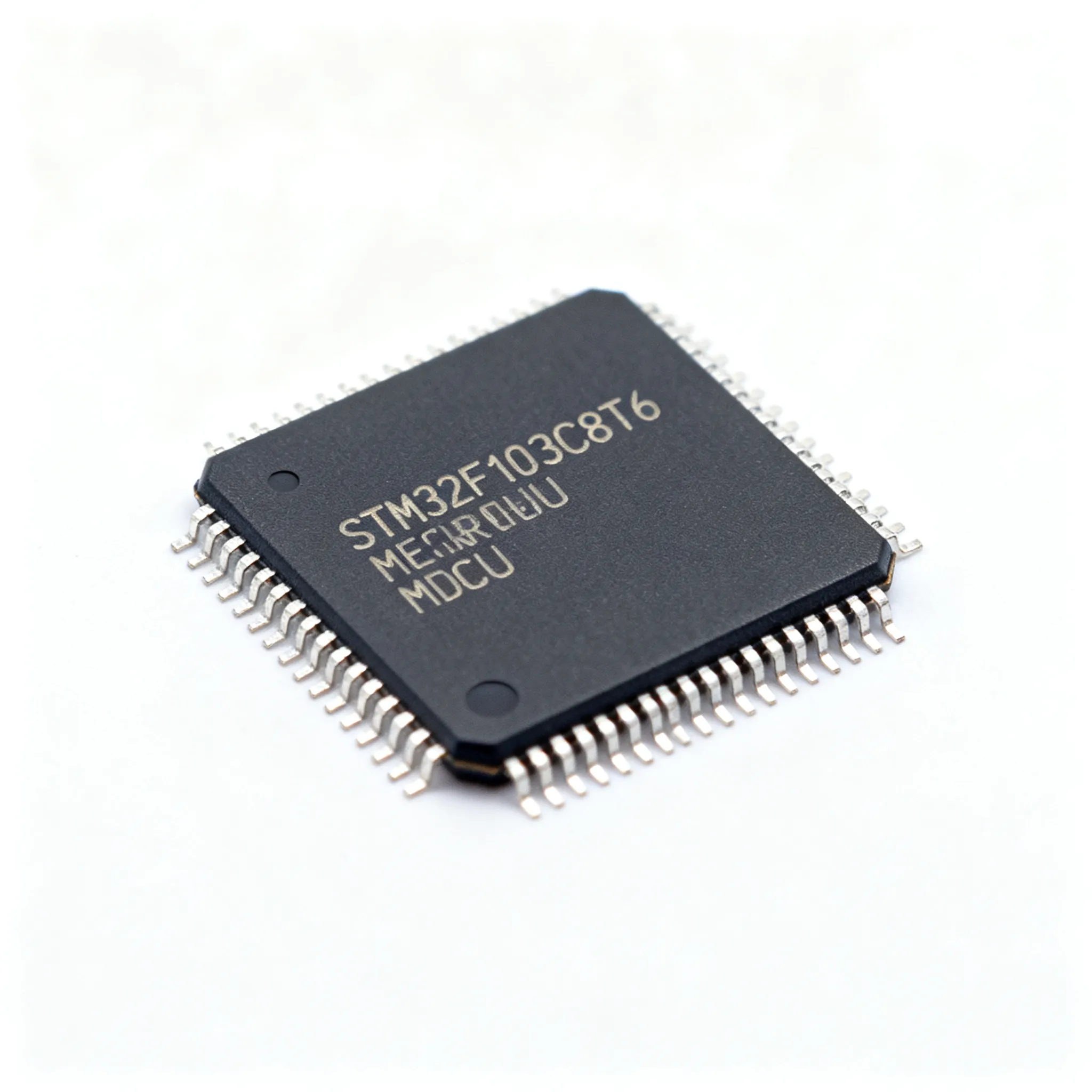
The STM32F103C8T6 comes in a 48‑pin LQFP package with a 0.5 mm pitch. The pinout organizes 37 GPIOs across five ports — PA0–PA15, PB0–PB15, and PC13–PC15 — with most pins offering up to three alternate functions. The SWD (Serial Wire Debug) interface occupies PA13 (SWDIO) and PA14 (SWCLK), so any design that needs debug connectivity must leave these two pins available. The main oscillator pins (PD0‑OSC_IN and PD1‑OSC_OUT) are shared with the high‑speed external clock, and the 32.768 kHz low‑speed oscillator maps to PC14‑OSC32_IN and PC15‑OSC32_OUT. Designers who skip these pinout details during schematic capture often discover that they have consumed a critical timer or ADC channel for a commodity function like an LED driver.
From a datasheet perspective, the electrical characteristics that matter most during design fall into a few categories: supply architecture, I/O DC parameters, ADC performance, and clock/reset behavior. The table below extracts the Tier‑A parameters that every design review should verify against the manufacturer's latest datasheet revision.
| Parameter | Value/Range | Unit/Notes |
|---|---|---|
| Operating voltage (VDD) | 2.0 to 3.6 | V; ADC and I/O performance degrade below 2.4 V |
| Core supply (internal regulator) | 1.8 | V; supplied by internal voltage regulator |
| Maximum CPU frequency | 72 | MHz; PLL sourced from HSE or HSI |
| Flash memory | 64 | KB; organized as 64‑bit wide access |
| SRAM | 20 | KB; includes 4 KB battery‑backed |
| I/O count (LQFP‑48) | 37 | GPIOs; 5‑V tolerant on most pins |
| ADC resolution / channels | 12‑bit / 10 external | 2 ADCs; up to 1 MSPS at 56 MHz ADC clock |
| Timer resources | 3× 16‑bit GP, 1× PWM, 2× watchdog, 1× SysTick | Advanced‑control timer for motor control |
| Communication interfaces | 2× SPI, 2× I²C, 3× USART, 1× USB 2.0 FS, 1× CAN 2.0B | USB and CAN share SRAM buffer |
| Temperature range (standard suffix) | −40 to +85 | °C; extended range available with different suffix |
| Package | LQFP‑48 (7 × 7 mm) | 0.5 mm pitch; RoHS compliant |
The ADC specification deserves particular attention. The two 12‑bit successive‑approximation ADCs in the STM32F103C8T6 can operate in dual mode, delivering up to 1 MSPS when the ADC clock is driven at 56 MHz. However, the effective number of bits (ENOB) degrades as the ADC clock approaches its maximum, and the datasheet specifies performance at a 14 MHz ADC clock for guaranteed accuracy. Designers who push the ADC to its timing limit without verifying the signal‑to‑noise ratio in their specific board layout often see unexpected LSB toggling. The AIChipLink guide reinforces this point: understanding the pinout and its interaction with analog routing is critical before committing to PCB layout³.
The I/O structure is another area where datasheet diligence pays off. Most GPIOs on the STM32F103C8T6 are 5‑V tolerant in input mode, but the output drive is limited to 8 mA per pin with a total IVDD + IVSS current limit of 150 mA across all supplies. Exceeding the total current budget can cause ground bounce that corrupts ADC readings or triggers spurious resets. The Utmel reference highlights the peripheral complement — two I²C, two SPI, three USARTs, USB, and CAN — and notes that the availability of these interfaces on specific pins is constrained by the LQFP‑48 package⁴. You cannot have all interfaces active simultaneously without careful pin‑function mapping; the alternate‑function table in the datasheet is the definitive reference for resolving conflicts.
Typical Boards and Peripherals Built Around STM32F103C8T6
The STM32F103C8T6 owes much of its visibility to the "Blue Pill" development board, a minimalist breakout that pairs the MCU with an 8 MHz external crystal, a 32.768 kHz oscillator, a micro‑USB connector, and a 3.3 V LDO regulator. The Blue Pill has become a de‑facto reference design for quick prototyping, and its schematic is widely circulated. However, the board's simplicity also exposes the MCU's pinout directly to the user — every GPIO, every power‑rail bypass capacitor, and the SWD header are brought out to 2.54 mm‑pitch headers. That makes the board a convenient vehicle for verifying pinout assumptions before committing to a custom PCB.
Beyond the Blue Pill, the STM32F103C8T6 appears in a range of application‑specific carrier boards. Motor‑control shields pair the advanced‑control timer with three‑phase inverter drivers, leveraging the timer's complementary PWM outputs and dead‑time insertion. CAN‑bus interface boards use the on‑chip bxCAN controller to implement nodes for industrial automation and automotive diagnostics. USB data‑acquisition modules exploit the full‑speed USB device peripheral to stream ADC data to a host PC at rates up to 12 Mbps. Each of these use cases stresses a different subset of the pinout and peripherals, which is why the datasheet's alternate‑function mapping table is the single most‑consulted page during board bring‑up.
| Peripheral / Interface | Typical Application | Key Pinout Considerations | Datasheet Reference Section |
|---|---|---|---|
| USB 2.0 Full Speed | Data loggers, firmware updates, HID devices | PA11 (USB_DM), PA12 (USB_DP); requires 48 MHz clock via PLL from HSE | USB peripheral section, clock tree |
| CAN 2.0B | Industrial gateways, OBD‑II interfaces | PB8 (CAN_RX), PB9 (CAN_TX) or alternate remap; external transceiver required | bxCAN section, AFIO remap table |
| ADC dual‑mode | Power monitoring, multi‑channel sensor arrays | PA0–PA7, PB0–PB1; VREF+ decoupling critical; avoid noisy digital traces near analog inputs | ADC characteristics, pin definitions |
| Advanced‑control timer (TIM1) | 3‑phase BLDC / PMSM motor control | PA8–PA11 (CH1–CH4), PB13–PB15 (complementary outputs); dead‑time insertion configurable | TIM1 section, alternate function map |
| I²C (2×) | EEPROM, sensor, and display interfaces | PB6‑PB7 (I2C1 default), PB10‑PB11 (I2C2); 4.7 kΩ pull‑up to 3.3 V typical | I²C characteristics, pin definitions |
| SPI (2×) | Flash memory, LCD controllers, RF modules | PA5‑PA7 (SPI1), PB12‑PB15 (SPI2); NSS can be software‑managed | SPI section, pin definitions |
What is striking about the STM32F103C8T6 is how much peripheral density STMicroelectronics achieved in a 48‑pin package. The trade‑off is that many peripheral functions share pins, and the designer must make deliberate choices early in the schematic phase. The Ultralibrarian article on the part notes that the standard "C8T6" suffix covers the −40 to +85 °C temperature range, while an extended temperature variant exists for industrial deployments that demand −40 to +105 °C operation⁵. Confirming the correct suffix before ordering is a non‑negotiable step, and the datasheet's ordering information table is the authoritative source.
Design and RFQ Checks Before You Source STM32F103C8T6
Sourcing the STM32F103C8T6 requires more than a part number on a purchase order. The part's longevity and wide adoption mean that legitimate supply exists across multiple channels, but the same factors also attract remarketed, re‑balled, or date‑code‑erased devices. The checklist below is intended as a practical framework for both design engineers and procurement buyers — it bridges the gap between the datasheet specification and the commercial reality of securing allocation.
Key RFQ and Design Verification Checklist:
- Verify the exact ordering suffix. The
STM32F103C8T6suffix encodes the temperature range (−40 to +85 °C), package (LQFP‑48), and Flash size (64 KB). Ordering a similar‑looking STM32F103xxx variant without confirming the suffix can land you a device with half the Flash or an incompatible footprint. Cross‑reference the datasheet ordering information table every time. - Request date‑code disclosure and a test report within 90 days. Buyers should require the distributor to provide a date‑code breakdown and a functional test report no older than 90 days. This is not a statement about current supply quality — it is standard procurement hygiene for a high‑runner MCU that has been in production for many years.
- Confirm allocation‑backed lead time via RFQ. Do not assume a standard lead time. The
STM32F103C8T6has experienced allocation tightening during periods of high demand across the STM32 family. Ask the supplier to confirm whether the quoted lead time is allocation‑backed or indicative, and request a written confirmation. - Validate the pinout against your schematic revision. Before releasing a PO, pull the latest STM32F103x8/xB datasheet and compare the alternate‑function mapping against your schematic. A single pin‑function conflict discovered after assembly can delay a production run by weeks. This is a Tier‑A datasheet task, not a procurement afterthought.
- Evaluate single‑source risk. While the
STM32F103C8T6is manufactured by STMicroelectronics, families such as GD32F103, APM32F103, and CH32F103 are sometimes evaluated as candidates by design teams seeking architectural alternatives. These candidates are not drop‑in replacements; they require verification of package compatibility, pinout mapping, peripheral register behavior, and firmware toolchain support. Consult the manufacturer's documentation and errata for each candidate before qualifying. - Inspect for RoHS and REACH compliance. The datasheet confirms RoHS compliance for the standard LQFP‑48 package, but buyers should still request a current certificate of compliance with the shipment. Regulatory requirements change, and a certificate that was valid six months ago may not reflect the latest substance restrictions.
The comparison table below maps the STM32F103C8T6 against two alternative MCU families that design teams frequently evaluate. The intent is not to declare a "best" option but to highlight the parameters that must be verified when considering a candidate for a production design.
| Comparison Metric | STM32F103C8T6 (STMicroelectronics) | GD32F103C8T6 (GigaDevice) — Evaluation Candidate | Selection Criteria & Failure Boundary |
|---|---|---|---|
| Core | ARM Cortex‑M3 @ 72 MHz | ARM Cortex‑M3 @ 108 MHz (GD32F103) | Higher clock may require timing loop recalibration; verify peripheral clock dividers |
| Flash / SRAM | 64 KB / 20 KB | 64 KB / 20 KB (GD32F103C8) | Memory map and page‑erase timing differ; verify bootloader compatibility |
| Package | LQFP‑48 (7 × 7 mm) | LQFP‑48 (7 × 7 mm) | Footprint‑compatible; verify pin‑1 marking and pad layout |
| ADC | 2× 12‑bit, 1 MSPS | 2× 12‑bit, 1 MSPS (GD32) | Calibration registers and sampling time differ; validate ADC driver code |
| USB / CAN | USB 2.0 FS, CAN 2.0B | USB 2.0 FS, CAN 2.0B | Buffer descriptors and interrupt mapping may differ; verify firmware stack |
| Power consumption | ~36 mA (72 MHz running) | ~30 mA (108 MHz, GD32 figure) | Compare at equivalent frequency; verify standby and stop mode currents |
| Toolchain | STM32CubeIDE, Keil, IAR, GCC | GigaDevice IDE, Keil, IAR, GCC | Peripheral library APIs differ; firmware porting effort is non‑zero |
| Supply chain | Single source (ST); verify allocation via RFQ | Single source (GigaDevice); verify allocation via RFQ | Verify single‑source risk for both; maintain approved vendor list |
The GD32F103C8T6 from GigaDevice is the most commonly discussed evaluation candidate, and the Unibetter guide covers it alongside other alternatives¹. However, the comparison above makes clear that even a pin‑compatible package does not guarantee firmware compatibility. The Cortex‑M3 core is the same, but the peripheral register maps, clock tree, and Flash programming algorithms differ enough that a qualification cycle is mandatory. Buyers and engineers who treat any alternative as a "guaranteed drop‑in" without a full verification suite risk field failures that far outweigh the initial cost savings.
The Alldatasheet listing for the STM32F103C8T6 provides a quick reference for the datasheet's front‑page summary, but the full 67‑page document is where the electrical characteristics and alternate‑function tables reside⁶. Procurement teams should treat the datasheet as a living document — STMicroelectronics issues revisions that may tighten or relax a parameter, and the revision that was current when a design was qualified may no longer reflect the silicon you receive eighteen months later.
STM32F103C8T6 Datasheet and Pinout FAQ
Q: Where should I start when looking up the STM32F103C8T6 datasheet?
Start with the official STMicroelectronics product page for the STM32F103x8/xB family. The datasheet document number (DS5319) covers the medium‑density performance line, including the STM32F103C8T6. Third‑party aggregators such as Alldatasheet and reference guides from AIChipLink and Utmel are useful for quick access to pinout summaries and application notes³⁴, but always validate against the manufacturer's latest revision. The datasheet revision history is the first thing to check — silicon errata and electrical specification updates are documented there.
Q: Which STM32F103C8T6 pinout details matter most for PCB layout?
The power‑supply pin placement is the most critical layout constraint. The STM32F103C8T6 requires VDD (pins 9, 24, 36, 48), VSS (pins 8, 23, 35, 47), and VDDA/VSSA (pins 6, 7) for the analog domain. Each VDD pin must have a 100 nF ceramic bypass capacitor placed as close as possible to the pin. The VDDA supply should be filtered — a ferrite bead or a 10 Ω resistor in series with VDD followed by a 1 μF + 10 nF capacitor pair is a common practice. The SWD pins (PA13, PA14) must be accessible for debugging; do not repurpose them as GPIOs unless you are prepared to lose debug connectivity. The oscillator pins (PD0, PD1) and the 32.768 kHz pins (PC14, PC15) should be routed with minimal trace length and kept away from high‑speed digital signals.
Q: How do Flash, SRAM, and package options affect STM32F103C8T6 selection?
The STM32F103C8T6 is the 64 KB Flash / 20 KB SRAM variant in LQFP‑48. The same family includes the STM32F103CBT6 with 128 KB Flash and the STM32F103R8T6 in LQFP‑64 with the same 64 KB Flash but more I/O pins. For a design that needs more than 64 KB of code space, moving to the 128 KB variant is a natural step, but the STM32F103C8T6 remains the sweet spot for cost‑optimized designs where the firmware fits within the 64 KB boundary. The 20 KB SRAM is adequate for most real‑time control loops and communication stacks, but applications that allocate large DMA buffers or run a TCP/IP stack alongside CAN and USB may push the SRAM limit. The Ultralibrarian reference confirms that the temperature range is encoded in the suffix — the standard "C8T6" covers −40 to +85 °C, and buyers needing extended temperature should verify the correct suffix with the supplier⁵.
Q: What should buyers verify before issuing an RFQ for STM32F103C8T6?
Before issuing an RFQ, buyers should confirm the exact part number suffix, request a recent date‑code disclosure, and verify that the supplier can provide a certificate of conformance with the shipment. The STM32F103C8T6 is an active, high‑volume part, but supply is allocation‑sensitive. Buyers should ask the distributor to confirm whether the quoted lead time is allocation‑backed and whether the devices are sourced through authorized channels. Traceability documentation — including the original manufacturer's lot number and a test report within 90 days — should be a standard requirement. Finally, confirm that the package marking matches the datasheet specification; the Unibetter guide provides visual reference for the top‑side marking to help identify genuine STMicroelectronics devices¹. These steps are not optional — they are the baseline for a defensible procurement process on a high‑runner MCU.
References & Further Reading
- STM32F103C8T6 Microcontroller Guide — Datasheet, Pinout, Development Board, Price, Alternatives, and Applications | Unibetter
- STM32F103C8T6 Datasheet (PDF) — STMicroelectronics | Alldatasheet
- STM32F103C8T6 Datasheet, Pinout, Schematic, Pins, and Development Board — AIChipLink
- STM32F103C8T6 Microcontroller: Pinout, Datasheet, and Circuit | Utmel
- STM32F103C8T6 Datasheet: Explained | Ultralibrarian
- STM32F103C8T6 Datasheet Search Results | Alldatasheet
- STM32F103C8 — Official Product Page | STMicroelectronics
- IC-Online — Electronic Component Sourcing and RFQ Platform
Designing with the [sku:STM32F