Step-by-Step Guide to PCB Assembly and Inspection Methods
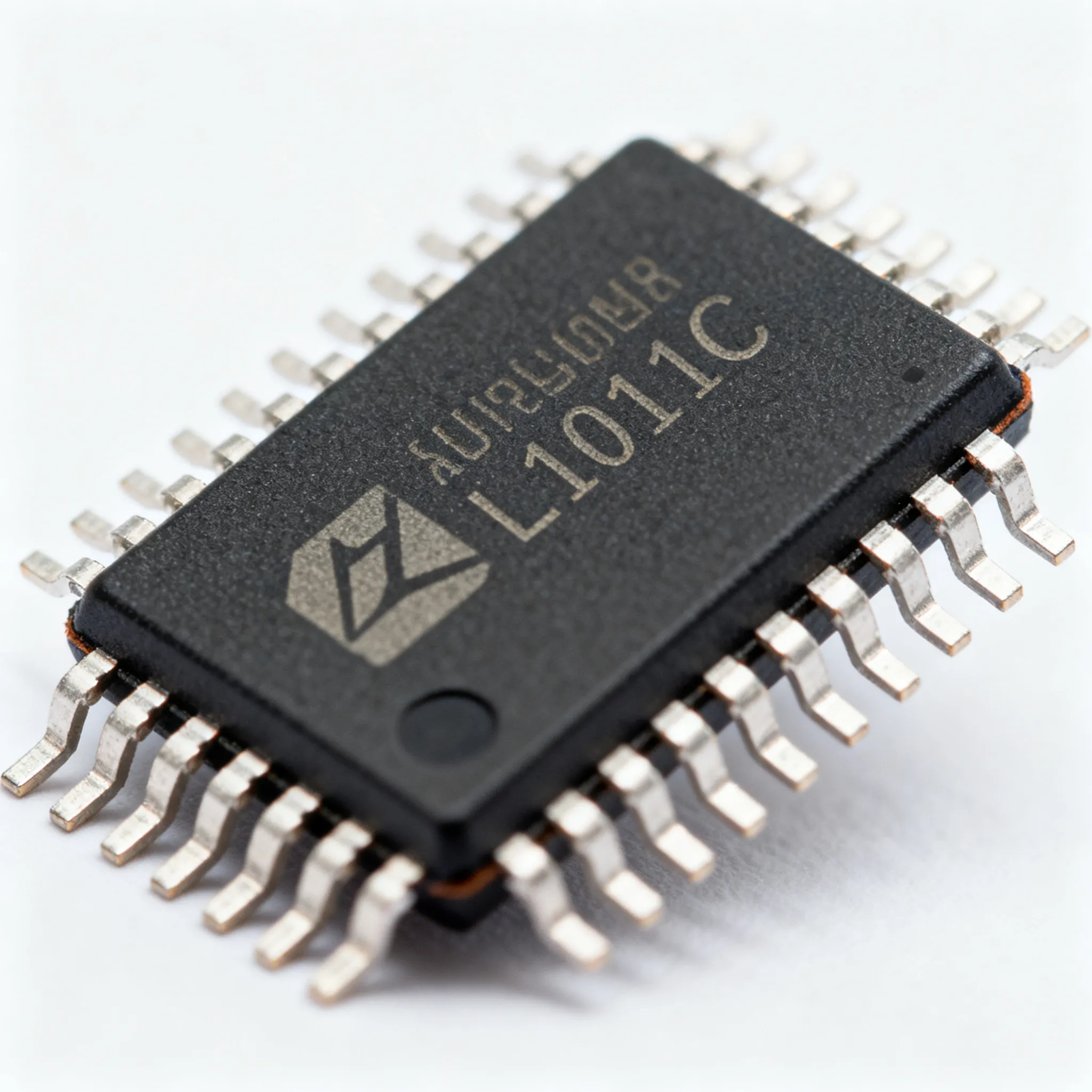
PCB assembly has many important steps. These include component inspection, solder paste inspection, and automated optical inspection. Each step in printed circuit board assembly needs careful quality control.
PCB assembly has many important steps. These include component inspection, solder paste inspection, and automated optical inspection. Each step in printed circuit board assembly needs careful quality control. This helps stop defects and makes sure the boards work well. Technicians use visual inspection, X-ray inspection, and in-circuit testing. These methods help find soldering problems, parts that are not lined up, and electrical faults. Checking the process often helps manufacturers find problems early. It also helps them keep high standards. By checking quality at every step, PCBA teams can make strong and high-quality printed circuit boards.
Key Takeaways
-
PCB assembly needs careful checks at each step to stop problems and make strong boards. Using machines like Automated Optical Inspection and X-ray helps find hidden issues early. Good design, correct part sourcing, and proper soldering help assembly work well and save time. Trained teams and clear process control keep quality high and lower mistakes. Using many inspection methods makes sure only good, working PCBs go to customers.
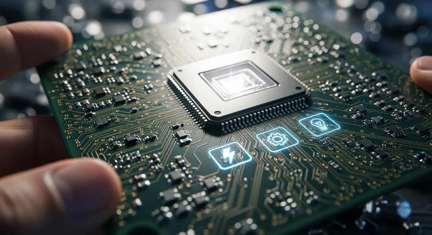
PCB Assembly Process
Printed circuit board assembly has many important steps. These steps help make sure the final product works well and lasts long. Each part of the process helps build a strong pcb. Surface Mount Technology and Through-Hole Technology are used in most modern pcb assembly. Surface Mount Technology lets machines put parts on the board quickly. Through-Hole Technology makes strong connections for parts that need to be tough.
Design for Assembly
Design for Assembly helps make pcb assembly go well. Engineers use simple designs to avoid problems. They pick standard parts and follow rules from the manufacturer. This helps stop mistakes and saves time. The design uses fewer through-hole parts, so drilling and assembly are faster. For Surface Mount Technology, designers keep at least 0.5 mm between parts and use the same pad sizes. For Through-Hole Technology, they check that holes are the right size. Using fewer parts and the same types makes assembly easier and lowers the chance of mistakes.
Tip: Do not change the design after making starts. This saves time and money.
Component Sourcing
Getting good parts is very important for pcb assembly. Teams pick suppliers who give full datasheets and show how long parts will last. They want to see if parts are real and can be returned if needed. Working with trusted suppliers helps when parts are hard to find. Tools like Octopart or TrustedParts help check prices and if parts are in stock. Picking the right parts at the start helps the assembly go well and makes sure the pcb works.
Solder Paste Application
Solder paste must be put on carefully to make strong joints. Technicians use stencils that are 0.1 mm to 0.15 mm thick. If there is too much paste, it can cause bridges. Too little paste makes weak joints. Checking the stencil and cleaning it often gives good results. Automated Optical Inspection and X-ray imaging check the solder paste. Keeping the right amount of paste helps make good connections and stops problems.
-
Stencil thickness: 0.1 mm – 0.15 mm
-
Solder joint fillet height: at least 25% of component end height
-
Placement deviation: not more than 50% of pad width
Component Placement
Machines put parts on the pcb in the right place. Sometimes parts are not lined up or are facing the wrong way. Technicians check the placement files and use marks to help line things up. Automated Optical Inspection, looking by eye, and X-ray inspection find mistakes. Good drawings with clear labels help stop errors. Putting parts in the right place helps the board work well and means less fixing later.
Reflow Soldering
Reflow soldering makes strong connections between parts and the pcb. The board goes through an oven that heats it in steps:
|
Temperature Range (°C) |
Duration / Rate |
Purpose / Notes |
|
|---|---|---|---|
|
Preheating |
120–160 |
1–3°C/sec rise rate |
Gets the board ready and stops damage from heat |
|
Insulation (Soak) |
120–160 |
60–100 seconds |
Keeps the board warm, helps clean the metal |
|
Reflow |
210–230 (Sn/Pb) |
20–30 seconds at peak |
Melts the solder paste; do not heat too long |
|
235–250 (Lead-free) |
Lead-free solder melts at about 217°C |
||
|
Cooling |
N/A |
3–10°C/sec cooling rate |
Hardens the solder joints; fast cooling makes strong bonds |
Controlling the oven makes sure the solder joints are good. Cooling the board right makes the joints strong and stops damage.
Through-Hole Assembly
Through-hole assembly means putting part leads into holes and soldering them on the other side. This is usually done by hand and is good for big parts that need to be strong. Through-hole parts are easy to fix or change, so this way is good for testing and tough jobs. But it takes more time and costs more than Surface Mount Technology. The choice depends on what the board needs to do and how many are made.
|
Aspect |
Through-Hole Assembly |
Surface Mount Assembly |
|---|---|---|
|
Component Mounting |
Put in holes, soldered on the other side |
Put on top of the board, soldered to pads |
|
Component Size |
Bigger parts |
Smaller parts, more can fit |
|
Assembly Process |
Soldered by hand |
Machines put parts and use an oven |
|
Repairability |
Easy to fix by hand |
Needs special tools |
|
Reliability |
Strong and can take heat |
Getting better, good for small boards |
|
Space and Weight |
Good for heavy-duty boards |
Best for light, mass-produced boards |
Cleaning
Cleaning takes off leftover flux and dirt after assembly. For small jobs, people use brushes and isopropyl alcohol. For big jobs, machines and ultrasonic cleaners do the work. The cleaning method depends on the type of flux used. Alcohol or special cleaners are for rosin and no-clean flux. Water is for water-soluble flux. Cleaning well stops rust and electrical problems, helping the pcb last longer.
-
Wet, scrub, rinse, and dry steps remove all dirt.
-
Safety means wearing gear and working where air moves well.
Final Inspection
Final inspection is the last check before sending out the board. Inspectors look at test results and records. They check for scratches, stains, or missing parts. Automated Optical Inspection and X-ray inspection find hidden problems. In-Circuit Testing and functional testing make sure the board works. Inspectors check if the board meets standards like IPC-A-610, ISO 9001, RoHS, and UL. The Quality Assurance team sorts problems as critical, major, or minor. Only boards that pass all checks are approved.
Note: Checking quality before and during assembly makes sure only good pcba boards go to customers.
Printed Circuit Board Assembly Technologies
Printed circuit board assembly uses two main ways: Surface Mount Technology and Through-Hole Technology. Each way changes how engineers plan, build, and check a pcb.
Surface Mount Technology (SMT)
SMT puts parts right on top of the pcb. Machines move fast and place small parts very carefully. This way makes boards smaller and lighter. It also lets engineers make more complex circuits. SMT lets parts go on both sides of the pcb. This gives more space for parts. Machines do most of the work, so SMT is quick and steady. This helps save money and stops mistakes.
|
Advantage |
Explanation |
|---|---|
|
SMT parts are tiny and light, so boards get smaller and lighter. |
|
|
Higher Connection Density |
More connections fit in one spot, so designs can be more complex. |
|
Double-Sided Mounting |
Parts can go on both sides, so there is more room. |
|
Faster and Easier Assembly |
Machines build SMT boards fast, which saves time and money. |
-
SMT does not need holes, so it uses less board space.
-
Pick-and-place machines help make the process faster and better.
-
SMT is good for high-frequency circuits because the leads are short.
-
This way also cuts down on waste and saves energy.
SMT makes checking boards with machines very important. Automated optical inspection and X-ray inspection are needed. These tools find problems like solder bridges and parts that are not lined up. They also find other mistakes that are hard to see.
Through-Hole Technology
Through-hole technology puts part leads through holes in the pcb. Then, they are soldered on the other side. This makes strong bonds, so it is good for parts that need to handle lots of power or stress. Big parts like capacitors, switches, and connectors use this way.
|
Industry |
Application Areas |
|---|---|
|
Used in car control, engine systems, and radios. |
|
|
Aerospace |
Used in plane controls, navigation, and radios. |
|
Industrial machinery |
Used in automation, motor drives, and power supplies. |
|
Medical devices |
Used in patient monitors and medical tools. |
|
Telecommunications |
Used in switches, routers, and base stations. |
|
Consumer electronics |
Used in amplifiers, power supplies, and connectors. |
|
Instrumentation |
Used in oscilloscopes, meters, and data loggers. |
Through-hole assembly is still needed for things that must be tough and last long. Engineers pick this way for test boards, fixing boards, and places with lots of shaking or heat. The strong solder joints help stop problems in hard jobs.
Note: Through-hole technology is easier to check by hand, but it takes longer than SMT. Inspectors use their eyes and in-circuit testing to find problems.
Both SMT and through-hole ways are important in pcb assembly. The best way depends on what the product needs, its size, and how strong it must be.
PCB Quality Control Methods
Printed circuit board assembly uses many ways to check quality. These methods make sure every board meets strict rules. Inspection and testing help find problems early. This stops big failures and saves money. Each method looks for certain issues. Using more than one inspection step keeps boards reliable. The table below shows the most common pcb quality control methods and what problems they find:
|
Quality Control Method |
Objective |
Defects Targeted |
|---|---|---|
|
Visual Inspection |
Manual check for obvious defects such as solder bridges and misaligned components. |
Visible assembly defects |
|
Automated Optical Inspection (AOI) |
Automated camera-based inspection to detect soldering defects and component placement errors. |
Soldering defects, component misalignments |
|
X-ray Inspection |
Reveals hidden or internal defects not visible to the naked eye. |
Solder voids, bridges, missing solder, misalignments |
|
Solder Paste Inspection (SPI) |
Checks solder paste volume and placement before component mounting. |
Insufficient/excess paste, misprints |
|
In-Circuit Testing (ICT) |
Measures electrical parameters and verifies correct component placement. |
Shorts, opens, wrong values, placement errors |
|
Functional Testing |
Simulates real-world operation to verify device performance. |
Functional failures, integration issues |
|
Flying Probe Testing (FPT) |
Flexible electrical testing for prototypes and small batches. |
Shorts, opens, misalignments |
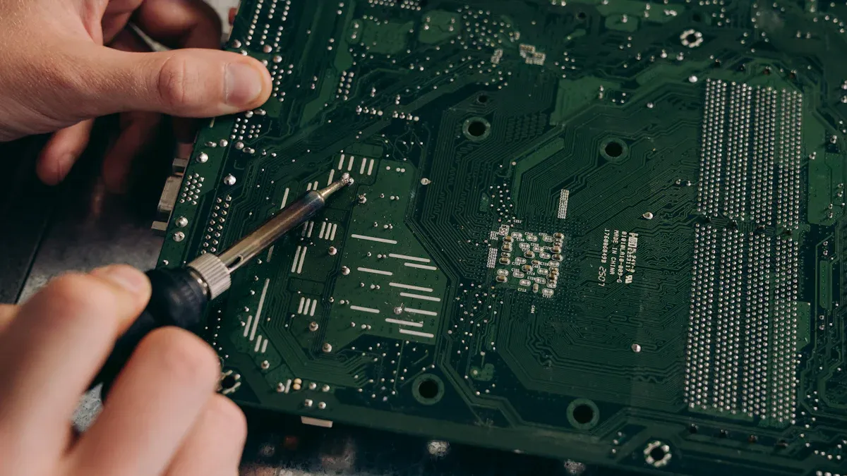
Visual Inspection
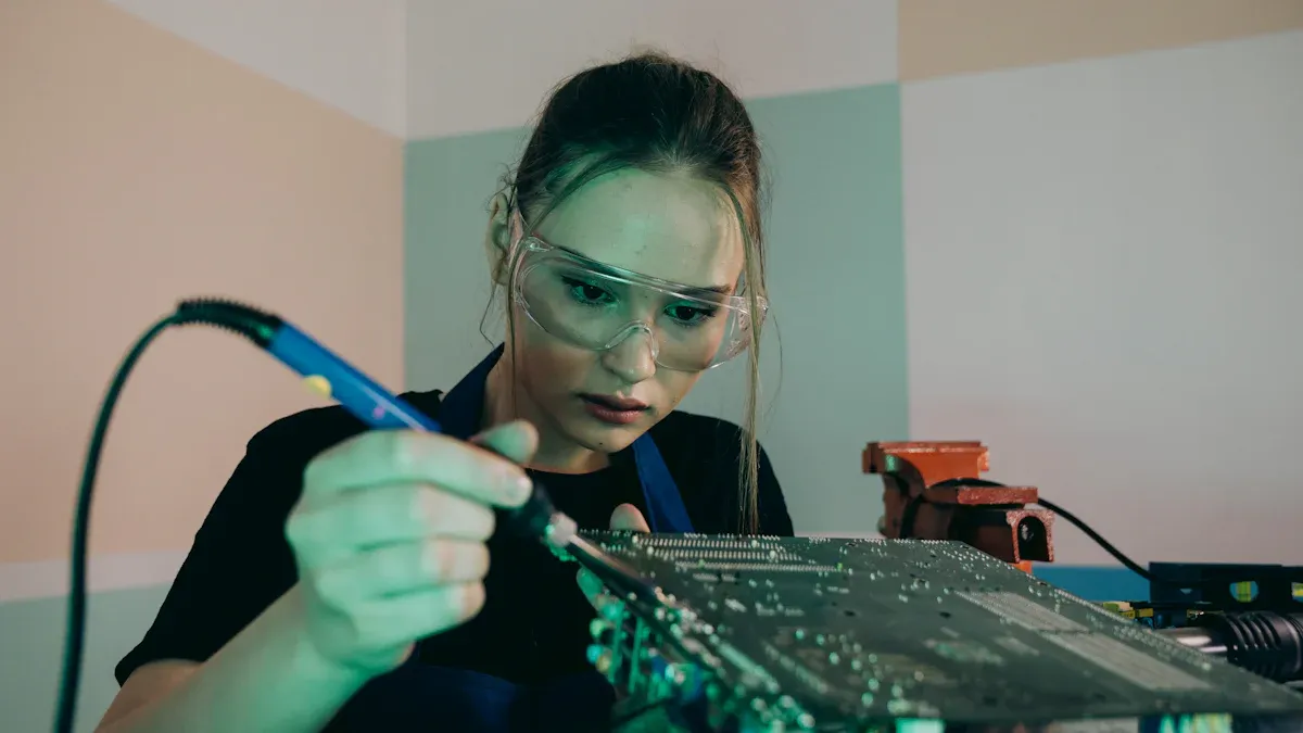
Visual inspection is a basic step in pcb quality control. Inspectors use magnifiers and microscopes to look for problems. They check for solder bridges, cold joints, missing or crooked parts, and dirt. Visual inspection happens after big steps like soldering and cleaning. This method works best for simple boards or as the first check. But people can miss small or hidden problems, especially on busy boards.
Tip: Using visual inspection with machines helps find more problems and lowers mistakes.
Automated Optical Inspection (AOI)
Automated Optical Inspection (AOI) uses cameras and smart software to scan the pcb for problems. AOI systems are very accurate and see things people cannot. They check thousands of parts every minute. AOI finds soldering problems, missing or wrong parts, polarity mistakes, and not enough solder. Factories use AOI after putting on solder paste and after reflow soldering. AOI lowers the number of missed problems by up to 90% compared to people checking. It gives quick feedback so workers can fix things right away. This method helps more boards pass and saves money by catching problems early.
-
-
Solder bridges and open spots
-
Parts that are not lined up
-
Missing or wrong parts
-
Polarity and direction mistakes
-
Note: AOI cannot see inside the board, so it works best with other checks.
X-ray Inspection
X-ray inspection is great for finding hidden or inside problems in pcb assemblies. This method is important for testing BGAs, QFNs, and boards with many layers. X-ray systems show solder voids, pin hole fills, solder bridges, missing solder, and crooked parts. They also find cracks in vias and problems inside the board. Inspectors use X-ray after reflow soldering or when boards have hidden joints.
Common problems found by X-ray inspection are:
-
Solder joint holes and air bubbles
-
Solder bridges between pads or balls
-
Not enough or missing solder
-
Pin hole fill problems
-
Inside cracks and layers coming apart
Solder Paste Inspection (SPI)
Solder Paste Inspection (SPI) checks the amount, height, and spot of solder paste before putting on parts. SPI uses 3D pictures to measure paste on each pad. This step stops problems like not enough solder, too much paste, and printing mistakes. These problems can cause solder bridges or weak joints. SPI happens right after stencil printing and before placing parts. By finding paste problems early, SPI helps keep pcb assembly quality high and cuts down on fixing mistakes.
-
SPI finds:
-
Too much or too little solder paste
-
Paste in the wrong place or missing
-
Stencil printing mistakes
-
In-Circuit Testing (ICT)
In-Circuit Testing (ICT) gives a full electrical check of finished pcbs. ICT uses a bed of nails or probes to touch test points on the board. The system checks resistance, capacitance, and if parts are in the right place. ICT looks for open circuits, shorts, wrong values, and correct voltage and current. This method is best for making lots of boards and for analog circuits. Test points and lines are put in smart spots to make sure signals are good and all parts are checked.
-
ICT checks:
-
Shorts and open spots
-
Resistance and capacitance numbers
-
Voltage and current at key places
-
Right placement and direction of parts
-
ICT is a main part of pcb quality control in big factories, making sure every board meets electrical rules.
Functional Testing
Functional testing acts like real use to make sure the pcb works right. Testers give power and signals, then watch outputs to see if things work. This method finds problems with how the board works, how parts work together, and hidden problems that other checks miss. Functional testing often uses stress and heat tests to see if the board lasts a long time. Studies show that functional testing lowers failure rates a lot, so it is very important for pcb assembly quality control.
-
Functional testing checks:
-
Logic and how the system works together
-
Power and signal strength
-
How the board handles stress from the environment
-
Functional testing is the last check, making sure only good pcbs go to customers.
Flying Probe Testing (FPT)
Flying Probe Testing (FPT) gives flexible and cheap electrical testing for new designs and small batches. FPT uses moving probes controlled by software, so no special tools are needed. This method changes fast for new designs and works with both surface mount and through-hole parts. FPT finds shorts, open spots, crooked parts, and wrong values. It covers a lot and is very accurate, so it is great for testing new boards and making changes quickly.
-
FPT is good because:
-
No special tools are needed
-
Fast to set up for new boards
-
Very accurate for tricky circuits
-
Does not hurt the board and can be done again
-
FPT fits well with pcb assembly, helping fast changes and strong pcb quality control.
Summary Table: PCB Quality Control Methods and Defects Detected
|
Method |
When Used |
Defects Detected |
|---|---|---|
|
Visual Inspection |
After major assembly steps |
Solder bridges, misalignments, visible errors |
|
AOI |
After solder paste and reflow |
Soldering defects, missing/misplaced components |
|
X-ray Inspection |
After reflow, for hidden joints |
Voids, bridges, missing solder, internal defects |
|
SPI |
After solder paste application |
Insufficient/excess paste, misprints |
|
ICT |
After assembly, before shipment |
Shorts, opens, wrong values, placement errors |
|
Functional Testing |
Final stage, before delivery |
Functional failures, integration issues |
|
Flying Probe Testing |
Prototypes, small batches |
Shorts, opens, misalignments, value errors |
Checking at many steps is key for good pcb quality control. Using these quality control methods together helps find problems early, makes checks strong, and only sends good boards to customers.
PCB Assembly Quality Control Best Practices
Keeping pcb assembly quality control high means following good steps. Teams need to watch the process, have trained workers, keep good records, and pick the right partners. These best ways help companies stay up to date and make products that work well.
Process Control
Process control is very important for pcb quality control. Teams check every step, like solder paste printing and reflow soldering. They set the right temperatures and take care of machines to stop problems. Workers use good solder paste and watch squeegee pressure to spread it evenly. Tools like AOI, X-ray, and SPI help find problems early. Systems watch temperature and humidity all the time. This helps teams see patterns and make quality better. Training and clear rules help people make fewer mistakes and keep quality control strong.
-
Set the best reflow soldering heat and keep machines working.
-
Use good solder paste and check how it is printed.
-
Make rules for work and train workers.
-
Use machines to check for problems.
-
Watch important things and look at problem data.
Skilled Teams and Training
Having trained workers is key for pcb assembly quality control. Companies pay for classes like IPC J-STD-001 Certification. These classes teach how to solder, find problems, and follow rules. Courses from Altium and others help engineers learn new things. Training helps workers do better, make fewer mistakes, and keep quality high. Certified teams can find and fix problems fast, so pcb quality control stays strong.
Documentation
Good records help track and check quality. Teams make clear BOMs, drawings, and plans. They write down how to test and what counts as passing. Version control keeps changes and records up to date. Barcodes and RFID tags help follow parts and boards. MES systems collect data and link it to each board. These steps make sure every pcb meets quality rules and helps with better quality control.
Outsourcing Considerations
Outsourcing can help pcb assembly quality control if companies pick good partners. Teams should check if partners have the right certificates and good checking systems. Good partners use AOI, X-ray, and watch the process in real time. They also work on getting better and keeping quality high. Talking clearly and keeping good records helps stop mistakes. Working together as partners, not just buyers and sellers, gives better results and stronger quality control.
Tip: Companies that use these best ways have fewer problems, spend less money, and make better products.
Common Defects and Prevention
Printed circuit board assembly can have many problems. These problems can make the board not work well or break early. Careful checking and good steps help teams find and fix these problems fast.
Soldering Defects
Soldering defects are some of the most common problems in PCB assembly. These problems include gaps in solder joints, solder balling, cold solder joints, solder bridging, and tombstoning. Each problem happens for a different reason and can hurt the board.
|
Defect |
Causes |
Effects |
|---|---|---|
|
Solder Bridging |
Too much solder paste, parts not lined up |
Short circuits, device stops working |
|
Cold Solder Joints |
Not enough heat, not enough flux |
Weak, easy-to-break connections |
|
Solder Balling |
Dirty parts, too much heat |
Shorts, bad connections |
|
Tombstoning |
Uneven heat during reflow |
Open or short circuits |
|
Lifted Pads |
Too much heat, shaking |
Broken connections, hard to fix |
Tip: Machines like AOI and X-ray help find these soldering problems before boards leave the factory.
Component Placement Issues
Problems with placing parts can make the board not work or break. Some problems are parts not lined up, put on wrong, too close together, or not planned for heat. Pick-and-place machines and AOI help put parts in the right spot. Design checks and clear labels also help stop mistakes.
-
Parts not lined up can cause shorts or open circuits.
-
Too many parts close together make fixing hard.
-
Wrong direction means the board will not work.
-
Bad heat planning makes the board get too hot.
Modern PCB design tools and regular checks help teams find these problems early.
Electrical Faults
Electrical faults can be open circuits, short circuits, or wrong part values. These problems can happen from bad soldering, wrong part placement, or things like dust and water. In-circuit testing and functional testing help find these faults. Teams also watch for ESD damage, which can cause hidden problems.
-
Open circuits stop electricity from flowing.
-
Short circuits connect things that should not touch.
-
Wrong part values change how the board works.
How Quality Control Prevents Defects
Quality control uses many checks and tests to stop problems. AOI looks for missing or wrong parts and soldering problems. X-ray finds hidden solder problems. In-circuit testing checks for shorts and open spots. Good steps, good materials, and trained teams all help stop common problems. By using these checks at every step, companies make strong and good PCBs.
Note: Checking early and often is the best way to stop expensive problems and make sure boards work well.
Each step in PCB assembly must be checked closely. Good quality control is very important. Teams that use the best ways find fewer problems. They also get better boards. They pay attention to new ideas in inspection and assembly tools. These new ideas help them work faster and make better boards. Learning about new PCB trends helps teams build stronger boards. Watching for new trends helps companies stay ahead of others.
FAQ
What is the most common inspection method in PCB assembly?
Visual inspection is used the most. Technicians look at boards with magnifiers or microscopes. They search for problems they can see. This step helps find issues early. It happens before machines check the boards.
Why do manufacturers use Automated Optical Inspection (AOI)?
AOI finds soldering and placement mistakes fast. Machines use cameras to scan the board. They compare pictures to design files. AOI makes checks more accurate. It also lowers mistakes made by people.
How does X-ray inspection help with quality control?
X-ray inspection shows hidden problems inside solder joints and under parts. It finds voids, bridges, and parts that are not lined up. Visual checks cannot see these problems. This method helps make sure complex boards work well.
What standards guide PCB assembly quality?
Manufacturers follow rules like IPC-A-610, ISO 9001, RoHS, and UL. These rules set how to build, keep safe, and protect the environment. Following these rules helps make boards the same quality every time.
Can PCB defects be repaired after inspection?
Yes, technicians can fix many problems. They use soldering tools to repair joints or change parts. Some big problems may mean the board cannot be fixed.
Tip: Finding and fixing problems early saves time and money in PCB making.