EV Charging Station BOM Guide: Power Semiconductors, Controllers, and Supply Risk
EV Charging Station BOM Guide: Power Semiconductors, Controllers, and Supply Risk
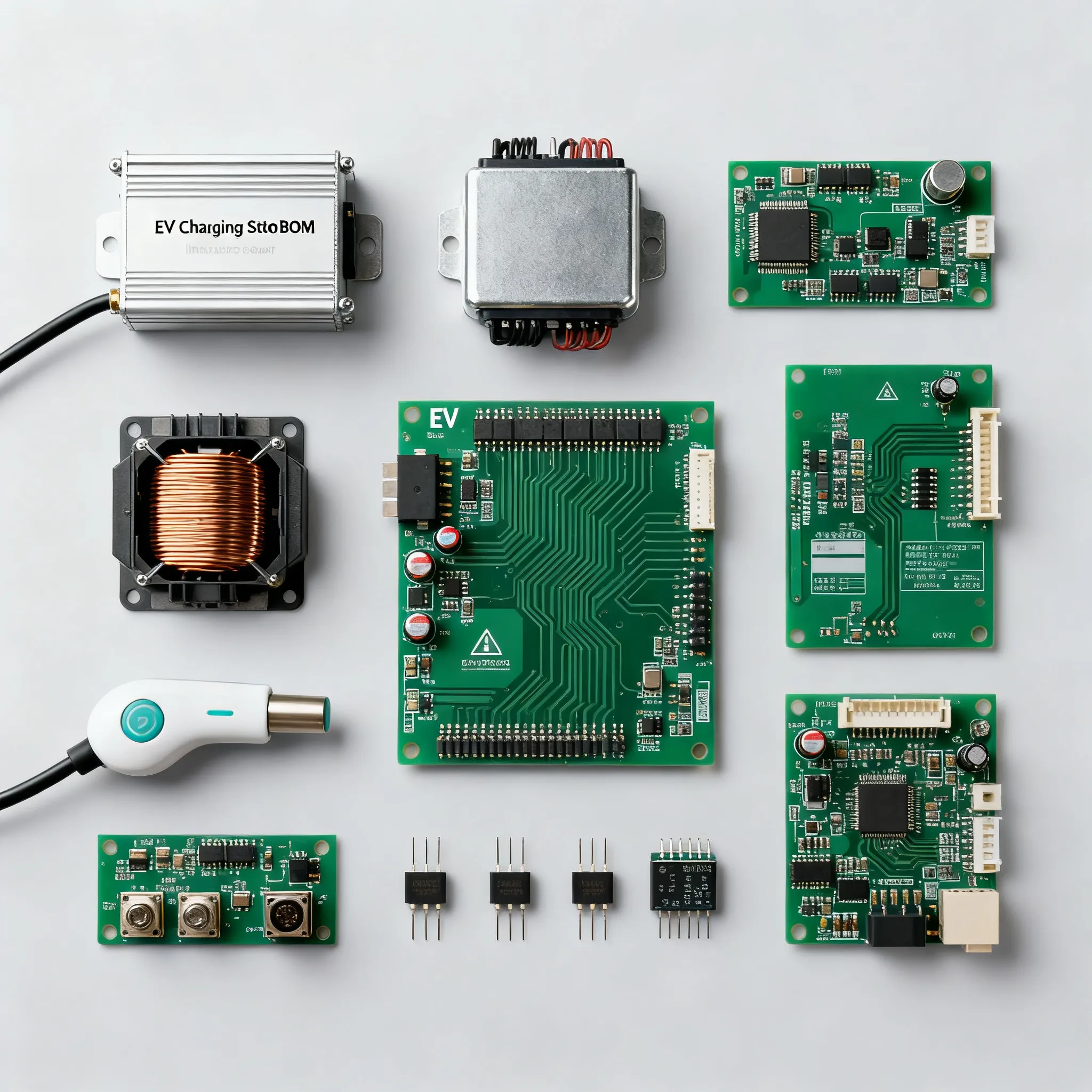
Why Power Semiconductor Lead Times Are Reshaping EV Charger BOMs
The semiconductor supply chain is no longer the frenzied free-for-all of 2021–2023, but for engineers and procurement teams building EV charging stations, the calm is deceptive. Demand for power semiconductors—the silicon, silicon carbide (SiC), and IGBT devices that sit at the heart of every Level 2 and DC fast charger—continues to outpace fab capacity expansions. This mismatch is quietly reshaping bill-of-materials (BOM) strategies, forcing you to look beyond simple unit cost and focus on availability, allocation, and second-source qualification.
According to J2 Sourcing’s lead-time data, automotive-grade MCUs from major suppliers like NXP, Microchip, Renesas, Infineon, and STMicroelectronics have stretched to 40–50 weeks during recent disruptions, and while conditions have improved, power discretes and modules are still in a state of managed allocation. The Utmel 2026 power semiconductor shortage outlook reinforces this: high-voltage components—specifically those operating at 48 V and above—are flagged as high-risk, and sourcing teams are being urged to treat them with the same urgency as they did microcontrollers during the chip crisis.
What does this mean for your EV charger BOM? The days of designing around a single, preferred supplier for a 1200 V SiC MOSFET or a high-side gate driver are fading. You need a proactive BOM strategy that identifies high-risk power-path components early, monitors lead-time trends continuously, and has pre-qualified alternatives before you get trapped in allocation. The table below highlights the key drivers that are reshaping this landscape.
| Driver | Mechanism | Procurement Impact |
|---|---|---|
| SiC fab capacity lag | Global SiC wafer and epitaxy supply remains concentrated; new fabs ramp slowly | Makes popular 1200 V SiC MOSFETs allocation items; forces multi-source qualification |
| Automotive electrification demand | EV traction inverters and on‑board chargers consume huge volumes of SiC and IGBT discretes/modules | Charger OEMs compete with automotive Tier 1s for the same part numbers; lead times extend |
| Wide-bandgap transition | SiC adoption in DC fast chargers increases; IGBTs remain in legacy designs | Designers must balance efficiency gains against supply risk of newer SiC products |
| MCU feature integration | Charge controllers absorb safety, security, and FOTA functions, making them less interchangeable | Single-sourced MCUs become critical path items; 40‑week lead times stall production |
| Geopolitical and fab allocation | Export controls, regional fab investments, and foundry allocation policies alter availability | Procurement must diversify beyond a single geography; second-source qualification becomes mandatory |
Tip: Start your BOM review by mapping every component that touches the high‑voltage, high‑current power path. If a part operates above 48 V and handles more than a few amps, treat it as a supply‑risk item. The Utmel risk matrix provides a clear workflow—Identify, Assess, Qualify—that you can apply immediately.
The Power Path: Silicon, SiC, and Gate Drivers Inside a DC Fast Charger
To make smart sourcing decisions, you need to understand exactly where power semiconductors live in a DC fast charger and how their requirements differ from the on‑board charger (OBC) you might have designed for a vehicle. While an OBC must handle a wide battery voltage range—from less than 250 VDC up to 850 VDC as shown in the onsemi OBC systems guide—a standalone DC fast charger must deliver high power directly to the vehicle battery, often at 400 V or 800 V levels, with output currents exceeding 300 A for a 150 kW unit.
The power conversion chain inside a typical 150 kW DC fast charger consists of three major stages, each placing unique demands on the power semiconductors and their support components.
AC/DC front‑end: The grid connection (480 V three‑phase) is rectified and power‑factor‑corrected. This stage commonly uses 1200 V SiC MOSFETs or IGBTs in a Vienna rectifier or active front‑end topology. The choice of device directly affects efficiency and heat load. SiC MOSFETs switch at higher frequencies (50–100 kHz) with lower losses, while IGBTs are robust but limit frequency to 20 kHz or so, forcing larger magnetics.
DC/DC converter: The isolated DC/DC stage steps the DC bus voltage down to the vehicle’s battery voltage. Here, SiC MOSFETs are increasingly the norm because their fast switching and low reverse recovery charge reduce transformer size and improve efficiency. Gate drivers for these SiC MOSFETs must handle high dv/dt and provide reinforced isolation, making them a critical sourcing item.
Auxiliary power supplies: Low‑voltage rails (12 V, 5 V, 3.3 V) for the controller, communication modules, and cooling fans are derived from the DC bus. While these use standard silicon MOSFETs, they are still part of the BOM and can be overlooked. The onsemi DC fast charging solutions page illustrates reference designs that integrate these stages with power management ICs (PMICs) and isolated gate drivers.
Microcontrollers sit at the top of this power chain, orchestrating the control loops, safety monitoring, and communication. The Renesas market trends blog highlights how modern MCUs for EV chargers are absorbing functions that once required separate ICs—hardware security modules, functional safety monitoring, and FOTA (Firmware Over‑the‑Air) capability. This integration reduces BOM line items but concentrates supply risk into a single, highly specialized part. If that MCU goes on allocation, your entire charger is held hostage.
ABB’s fielded infrastructure, documented in their EV charging infrastructure documents, demonstrates how these architectures scale from 50 kW to 350 kW. In the field, the power semiconductor BOM is not just about performance—it’s about serviceability, thermal cycling, and long‑term availability. That’s why procurement teams are now involved at the architecture stage, not just when the design is frozen.
SiC, IGBT, or Superjunction? Matching Power Semiconductors to Charger Architecture
Choosing the right power semiconductor for each stage of an EV charger is a multi‑dimensional decision. You’re evaluating voltage rating, switching frequency, thermal performance, and—critically—supply resilience. The table below maps the most common options to typical charger positions and flags the supply‑risk factors that procurement teams should track.
| Segment / Option | Effect on BOM and Supply | Notes |
|---|---|---|
| 1200 V SiC MOSFET discrete | High efficiency, enables compact design; limited suppliers, allocation risk | Used in front‑end and DC/DC stages; multi‑source qualification essential |
| 1200 V SiC power module (half‑bridge, full‑bridge) | Simplified layout and cooling; often single‑source, high lead‑time risk | Common in 150 kW+ modules; verify second‑source or alternative module footprints |
| 1200 V IGBT module (with co‑packaged diode) | Mature technology, multi‑source possible; larger, lower frequency, more heat | Still used in cost‑sensitive designs; lead times more stable but watch for demand spikes |
| 650 V Superjunction MOSFET | Low on‑resistance for auxiliary power; broad supply base, low risk | Typical for low‑power auxiliary rails; rarely a supply bottleneck |
| Integrated power module (SiC + driver + protection) | Reduces component count, speeds design; single‑source, high specificity | Attractive for fast‑to‑market designs but increases procurement risk; onsemi technical documentation offers alternatives |
The Utmel risk matrix categorizes any component operating at 48 V and above as high‑risk, but in an EV charger context, the real vulnerability lies in the 1200 V class. These devices are heavily consumed by automotive traction inverters, and the same wafer starts that feed a DC charger module are also feeding a luxury EV’s rear drive unit. When automotive OEMs forecast aggressively, charger manufacturers get squeezed.
Controller choice compounds the risk. The J2 lead‑time data shows that many automotive‑grade MCUs still hover in the 40‑week range for popular families, and the Renesas blog confirms that integrating safety, security, and FOTA features into a single MCU is the industry direction. This means you can’t easily swap an NXP S32K for a Renesas RH850 without significant firmware rework. As a result, the MCU becomes a supply‑chain choke point. Smart BOM planners are not just comparing three‑phase PFC controller specs; they’re comparing the size and health of the supplier’s approved vendor list (AVL) for that MCU family.
When you need to explore alternative parts, onsemi’s technical documentation provides a searchable database of power discretes, modules, and gate drivers with parametric filtering. This is a practical starting point for identifying drop‑in or near‑drop‑in alternatives when your primary source is on allocation.
Building a Supply-Risk Buffer: AVL Expansion and Lead-Time Triggers for Power Components
Procurement leads and engineering managers often treat supply‑risk mitigation as a reactive exercise—something you do when a shortage hits. In the EV charger market, that approach is a recipe for stalled production. The following table outlines four concrete actions you can take now, when to apply them, and the trade‑offs involved.
| Action | When to Use | Trade‑off |
|---|---|---|
| Map BOM to isolate high‑voltage/high‑current power paths | At design concept stage, before supplier selection | Requires cross‑functional effort between engineering and procurement; adds 2–3 days to BOM review |
| Qualify pin‑compatible or functionally equivalent second sources | Before first prototype build, and continuously during production | May require additional qualification testing and minor layout adjustments; prevents single‑source lock‑in |
| Monitor lead‑time trends and set allocation triggers | Monthly, integrated into MRP/ERP systems | Needs disciplined data tracking; false alarms can cause unnecessary buffer stock |
| Evaluate OEM vs. ODM model for charger sub‑systems | When time‑to‑market is critical but safety/revenue is at stake | ODM offers faster deployment but you lose BOM control; Joint Charging’s guide warns that mixing OEM/ODM terms can create IP and safety risks |
The Utmel risk‑matrix workflow—Identify high‑risk components, Assess lead times and specifications, Qualify alternatives—is a practical framework you can start using today. Begin by marking every line item in the BOM that handles more than 48 V and carries significant current. Next, list the current lead time for each of those parts, using J2’s benchmarks as a reference. If a part’s lead time exceeds 26 weeks, flag it for immediate AVL expansion.
One common mistake is treating OEM and ODM relationships loosely. In the EV charger space, Joint Charging’s sourcing guide clarifies that these terms describe fundamentally different commercial arrangements. If you’re building a charger that affects safety or revenue—and most DC fast chargers do—you should maintain full BOM control. That means specifying the exact power semiconductor, gate driver, and MCU, and qualifying second sources yourself. Using an ODM for the entire charger may seem attractive, but you inherit the ODM’s supply chain risks without the visibility to manage them.
For gate drivers and PMICs specifically, use onsemi’s technical documentation to search for pin‑compatible alternatives. Many isolated gate drivers from different manufacturers share the same SOIC‑8 or SOIC‑16 footprint, but subtle differences in propagation delay, common‑mode transient immunity, and UVLO thresholds can break a design if not validated. Factor in the time to test these alternatives on your actual power stage—not just a bench evaluation board—so you’re not discovering a layout‑dependent issue during a shortage.
Power Semiconductor and Controller Sourcing: Questions Engineering Teams Ask
In the final section, we address the most common questions that come up when senior engineers and buyers sit down to plan an EV charger BOM. The answers draw directly from the cited sources and reflect the practical realities of a supply chain that remains under pressure.
Q: What are realistic lead times for 1200 V SiC MOSFETs in 2026?
While lead times are improving from the 2022–2023 peaks, many popular SiC devices remain in the 20–30 week range, with some automotive‑qualified parts still stretching to 40+ weeks. The Utmel outlook recommends monitoring allocation closely and qualifying alternative sources early. You should expect that any SiC MOSFET with a AEC‑Q101 qualification will be longer‑lead than its industrial‑grade counterpart, simply because the automotive pipeline consumes most of the available wafers.
Q: How do I decide between discrete SiC MOSFETs and a power module for a 150 kW charger?
The decision involves trade‑offs in thermal management, scalability, and supply flexibility. Discrete devices offer more sourcing options and allow you to fine‑tune the layout for parasitic inductance, but they demand more design effort in paralleling and gate‑drive optimization. Power modules simplify the mechanical and cooling design, but they are often single‑sourced and can be subject to severe allocation. onsemi’s DC fast charging solutions illustrate both approaches, and their OBC guide shows the voltage ranges that influence the choice. If you can afford to design and qualify a discrete‑based power stage, you gain a more resilient supply chain.
Q: Which microcontrollers offer integrated safety and FOTA for EV charging stations?
Renesas, NXP, Infineon, and STMicroelectronics all provide MCUs with hardware security modules, functional safety up to ISO 26262, and FOTA support. The Renesas blog highlights the trend toward integrating safety, security, and communication peripherals to reduce BOM, while J2’s lead‑time data underscores the need for dual‑sourcing these high‑demand parts. When evaluating an MCU, don’t just look at the feature set; ask the supplier for a 12‑month availability forecast and identify a second MCU family that can meet at least 80% of the functionality without a complete board respin.
Q: Are AEC‑Q qualified components mandatory for EV charging stations?
Not always, but many charger OEMs require automotive‑grade components for reliability and temperature range, especially in outdoor installations. AEC‑Q qualification can tighten supply, as seen in J2’s report, where automotive MCUs saw 40–50 week lead times. Industrial‑grade alternatives may be acceptable in non‑critical sub‑systems like auxiliary power supplies, but the Utmel risk matrix advises extra scrutiny for high‑voltage/high‑current paths. If you choose to use industrial‑grade parts in the power path, you must validate their performance over the charger’s full temperature and humidity range, and you assume the risk of reduced reliability margins.
Q: When should I consider an ODM charger instead of building my own BOM?
If in‑house power electronics expertise is limited and time‑to‑market is critical, an ODM solution can be faster, but Joint Charging’s guide warns that mixing OEM/ODM terms can lead to IP and safety risks. For any application where charger failure creates safety or revenue risk—such as a public 150 kW fast charger that generates income per session—you should maintain full BOM control. That means you define the power semiconductors, controllers, and gate drivers, and you qualify the supply chain yourself. ODM is more appropriate for low‑power, non‑revenue‑generating units where a failure is merely an inconvenience.
Q: How can I mitigate single‑source risk for gate drivers and PMICs?
Expand the approved vendor list (AVL) by qualifying pin‑compatible or functionally equivalent parts from multiple suppliers. Use onsemi’s technical documentation and the Utmel risk workflow to identify and assess alternatives before shortages occur. Also, leverage ABB’s infrastructure documents to understand typical component ratings and substitution requirements. For gate drivers, pay close attention to the isolated output drive current, propagation delay matching, and the common‑mode transient immunity (CMTI) specification—these are the parameters that differ most between suppliers and can cause subtle failures if not tested at the system level.
Need components or PCBA support for EV Charging Station products? IC-Online helps smart-device OEMs with sourcing and board-level supply — see our Smart Device Solutions or contact our team for a BOM review.
References & Further Reading
- Automotive semiconductors: AEC‑Q and lead times – J2 Sourcing
- Power Semiconductors Shortage Outlook 2026 – Utmel
- DC Fast EV Charging Solutions – onsemi
- onsemi On‑Board Charger Systems Solutions Guide – Avnet
- Market and Technology Trends for EV Charging Stations – Renesas
- EV Charging Infrastructure Documents – ABB
- Sourcing EV Chargers 2026: OEM vs ODM vs Private Label – Joint Charging
- Technical Documentation – onsemi
For procurement teams seeking flexible minimum order quantities and a broad line card, IC-Online provides access to mixed BOM solutions that can help you navigate the fragmented power semiconductor market. As you finalize your EV charger BOM, remember that the companies who treat supply‑risk assessment as a continuous design input—not a one‑time sourcing event—will be the ones who keep charging stations rolling off the line when the next allocation wave hits.