

IGBT vs MOSFET: Common Pitfalls in Gate Drive Design and How to Troubleshoot Them
Expert guide on IGBT vs MOSFET: Common Pitfalls in Gate Drive Design and How to Troubleshoot Them. Technical specs, applications, sourcing tips for engineers and buyers.
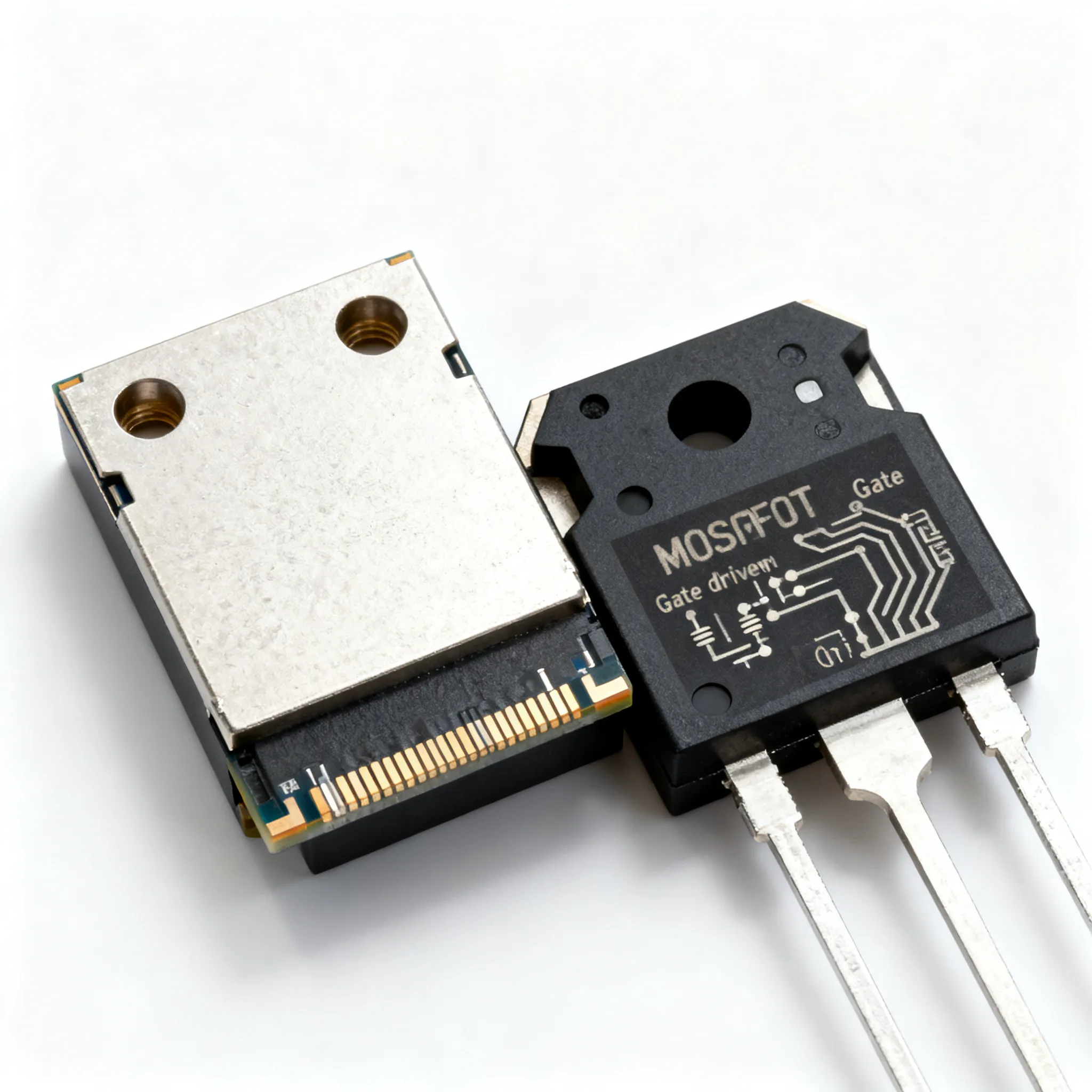
Why Gate Drive Design Is the Weakest Link in IGBT and MOSFET Reliability
When a 1200 V IGBT module fails catastrophically in a traction inverter, or a bank of MOSFETs self-destructs in a server power supply, the post-mortem rarely points to an intrinsic device defect. Instead, the root cause hides in the gate drive circuit—a handful of passive components and a driver IC that are often treated as an afterthought. In the last 12 months, updated failure analysis resources from Dynex (AN6442-2, July 2024) and Fuji Electric have catalogued the same recurring themes: mismatched gate resistors, insufficient dead time, and parasitic turn-on can destroy a device in seconds. A widely discussed EDABoard forum case illustrates the point perfectly—a seemingly simple incandescent lamp load driven by a MOSFET controlling an IGBT gate, with a rectified but unfiltered DC bus, produced a clean output waveform yet still destroyed the IGBT because the gate drive couldn’t cope with the high dv/dt and ringing.
EEWorldOnline reminds us that gate drivers are the critical link in power device performance, yet they are frequently overlooked until field returns start piling up. For engineers and procurement professionals alike, understanding the pitfalls of gate drive design isn’t just a technical curiosity—it’s a direct line to reliability, cost, and supply chain resilience.
How Gate Drive Circuits Differ Between MOSFETs and IGBTs (and Why It Matters)
Both MOSFETs and IGBTs are voltage-controlled devices, but treating them as interchangeable from a gate drive perspective is a recipe for disaster. Littelfuse’s AN-401 and ST’s AN524 make the distinction clear: a MOSFET’s gate behaves like a pure capacitor, and switching speed is determined by how quickly the driver can charge and discharge the gate capacitance. An IGBT, however, has a MOSFET-like input stage but a bipolar output, which introduces a tail current during turn-off. That tail current cannot be swept away by simply pulling the gate low; it must be managed with careful gate voltage shaping to minimize turn-off losses.
Parasitic turn-on—where high dv/dt on the collector or drain couples through the Miller capacitance and momentarily turns the device back on—is a threat to both device types. ROHM’s SiC gate drive design guidelines emphasize that even standard silicon MOSFETs are susceptible, and the problem becomes acute in fast-switching SiC circuits. IGBTs face the same challenge, particularly in half-bridge topologies where a shoot-through event can be lethal.
The table below captures the essential gate drive parameters that dictate driver selection and circuit topology for silicon MOSFETs and IGBTs. (SiC MOSFETs are included for reference, as they often appear in the same design conversations.)
| Parameter | Silicon MOSFET (e.g., 650 V) | IGBT (e.g., 1200 V) | SiC MOSFET (typical) | Drive Circuit Implication |
|---|---|---|---|---|
| On-state gate voltage (VGS/VGE) | 10–12 V | 15 V (±1 V) | +18 V (tightly regulated) | IGBTs need a higher plateau; SiC demands precise regulation to avoid gate oxide stress. |
| Off-state voltage | 0 V (or -5 V for dv/dt immunity) | 0 V to -15 V (common -8 V) | -5 V to -3 V (mandatory) | Negative bias is a safety margin for IGBTs; a must for SiC. |
| Gate threshold voltage (VTH) | 2–4 V | 4–6 V | 2.5–4.5 V | Low VTH increases susceptibility to Miller-induced turn-on. |
| Total gate charge QG (typical) | 20–100 nC | 100–500 nC | 30–120 nC | IGBTs require higher peak gate current to achieve fast switching. |
| Miller plateau voltage | 3–5 V | 8–10 V | 5–7 V | Driver must source/sink enough current to traverse the plateau quickly. |
| Peak gate current (IG) | 1–4 A | 2–8 A | 4–10 A | Higher current reduces switching losses but increases EMI. |
| Turn-off tail current | None | Significant (depends on carrier lifetime) | None | IGBT turn-off gate resistor must be optimized to balance tail loss and voltage overshoot. |
| dv/dt immunity requirement | Moderate (50 V/ns typical) | High (up to 50 V/ns) | Very high (>100 V/ns) | Active Miller clamp or negative voltage is essential for IGBTs and SiC. |
Tip: The numbers above are not datasheet maximums; they represent the driving conditions you must provide. Under-driving an IGBT gate (e.g., using a 10 V rail instead of 15 V) increases conduction losses and can push the device into linear operation, triggering thermal runaway. Over-driving a MOSFET gate beyond its rated ±20 V limit—even for nanoseconds—can puncture the gate oxide.
Side-by-Side Gate Drive Design Choices: MOSFETs vs. IGBTs in Real Circuits
When a design team sits down to choose between an IGBT half-bridge and a MOSFET-based solution, the decision tree extends well beyond conduction losses. The gate driver topology, its bill of materials (BOM), and the associated supply chain risk can tip the scales. IC-Online’s own sourcing guide confirms that IGBT modules often require isolated gate drivers with desaturation (desat) detection, while many MOSFET designs can leverage simpler bootstrap drivers. Kynix’s analysis is unequivocal: you cannot simply drop a MOSFET driver into an IGBT circuit and expect reliable operation. Utilities Bunker’s comparison stresses that total loss—not just RDS(on) or VCE(sat)—must dictate the final choice, and Hiitio’s SiC vs. IGBT study highlights the extreme voltage sensitivity of modern MOSFET gates, a factor that directly impacts driver BOM cost.
Below is a practical, buyer-friendly comparison that distills these trade-offs for a 3 kW–10 kW power stage operating at 20 kHz–100 kHz.
| Comparison Metric | IGBT Half-Bridge (Isolated Driver + Desat) | Si MOSFET Half-Bridge (Bootstrap Driver) | SiC MOSFET Half-Bridge (Dedicated Isolated Driver) | Selection Criteria & Risk Boundary |
|---|---|---|---|---|
| Typical gate driver IC | ACPL-33x, ISO5852S, 1EDI series | IR2110, UCC27714, NCP51530 | Si827x, NSi66x1A, UCC21750 | Isolation is mandatory for IGBT modules; functional isolation may suffice for discrete MOSFETs. |
| Negative voltage rail | Required for high dv/dt (often -8 V to -15 V) | Optional; 0 V with Miller clamp often sufficient | Mandatory (-5 V to -3 V) | Skipping negative bias on SiC MOSFETs risks gate oxide damage; on IGBTs it invites shoot-through. |
| Desaturation / short-circuit protection | Integrated or external desat circuit | Not typical; relies on current sensing elsewhere | Desat or fast overcurrent detection | IGBTs and SiC MOSFETs demand fast fault response; desat detection adds BOM cost but saves modules. |
| BOM cost per channel (relative) | High (isolated DC-DC, optocoupler/digital isolator, desat components) | Low (bootstrap diode, capacitor, single driver IC) | Medium–High (isolated gate driver, negative bias supply, clamping diodes) | A bootstrap driver lowers cost but limits duty cycle to <95% and cannot handle sustained high-side on-time. |
| Switching frequency range | 5–40 kHz (hard switching) | 50 kHz–200 kHz+ | 50 kHz–300 kHz+ | IGBTs are preferred at lower frequencies due to tail current losses; MOSFETs excel at high frequency. |
| dv/dt immunity | Good (when negative rail used) | Moderate (improved with active Miller clamp) | Excellent (with dedicated driver) | High dv/dt can falsely trigger the gate; choose a driver with CMTI >100 kV/µs for SiC. |
| Procurement lead time risk | High for isolated gate drivers (30+ weeks allocation) | Moderate (multi-sourced bootstrap drivers) | High, but pin-compatible alternatives exist (e.g., NSi66x1A) | Second-source qualification is essential; consider drop-in replacements early in the design phase. |
IGBT-based designs continue to dominate high-power, low-frequency applications such as motor drives and induction heating, where the ruggedness and low conduction losses at high current outweigh the switching limitations. MOSFETs, including SiC, are pushing into higher frequencies and higher power densities, but the tighter gate drive requirements demand a careful sourcing strategy. The availability of pin-compatible alternatives like the NSi66x1A-Q1—which integrates active pull-down and is automotive-qualified—gives buyers a much-needed lever when lead times stretch.
How to Troubleshoot and Prevent the Five Most Common Gate Drive Pitfalls
Field failures, whether in an IGBT-based welding inverter or a server MOSFET VRM, tend to cluster around a handful of gate drive mistakes. The Dynex and Fuji failure mode documents, together with Littelfuse and ST guidance, provide a clear diagnostic framework. The table below maps the five most frequent pitfalls to their symptoms, root causes, and field-tested fixes.
| Pitfall | Symptoms | Root Cause | Field-Tested Fix | Reference |
|---|---|---|---|---|
| 1. Gate ringing & parasitic turn-on | Unexplained shoot-through, excessive EMI, device overheating | High dv/dt couples through Miller capacitance, gate loop inductance causes oscillation | Use split gate resistors (RGon < RGoff), add a ferrite bead or gate resistor close to the gate pin, enable active Miller clamp or negative voltage | Littelfuse AN-401, ROHM SiC guidelines |
| 2. IGBT latch-up under load | Device destruction after a short overload, gate signal appears clean | Gate-emitter voltage drops below VTH while collector current is high, forcing the parasitic thyristor to latch | Ensure driver can sink >2 A peak current, maintain VGE plateau above 12 V during on-state, use a low-impedance gate discharge path | Fuji Electric failure modes, ST AN524 |
| 3. Gate oxide overvoltage (SiC MOSFETs) | Permanent gate-source short, reduced threshold voltage drift | Overshoot beyond +22 V or negative spikes below -10 V during switching | Use tightly regulated +18 V/-5 V supply, add 18 V Zener clamp from gate to source, select a driver with integrated active clamping | Hiitio SiC vs IGBT study, ROHM guidelines |
| 4. Incorrect gate resistor selection | Slow switching, high switching losses, or excessive voltage overshoot at turn-off | RG too large increases switching time; too small causes ringing and EMI | Start with datasheet RG curve, fine-tune by measuring VCE/VDS overshoot and dv/dt, use separate resistors for turn-on and turn-off | Dynex AN6442, Littelfuse AN-401 |
| 5. Loss of gate drive power during operation | Uncontrolled device turn-on, shoot-through when auxiliary supply fails | Driver VCC2 disconnected; gate floats or is pulled up by leakage | Use a driver with active pull-down (e.g., NSi66x1A-Q1), add a gate-source resistor (10 kΩ) as a fail-safe, monitor UVLO thresholds | NSI66x1A-Q1 datasheet, ST AN524 |
Beyond the table, three practical steps can prevent most gate drive failures before they reach the test bench:
- Measure, don’t guess. Use a differential probe with sufficient bandwidth (≥200 MHz) to capture the gate waveform directly at the device pins. A 1 cm lead length can add 10 nH of inductance, transforming a clean lab signal into a ringing mess.
- Validate under worst-case conditions. High-line voltage, maximum load, and cold temperature all increase dv/dt and gate charge demands. The Dynex application note recommends testing at 120% of nominal DC bus voltage with a clamped inductive load to simulate real stress.
- Design for fault tolerance. The NSi66x1A-Q1’s active pull-down feature is a perfect example: if VCC2 is lost, the gate is actively held low, preventing a floating condition that could turn on the power device and cause a catastrophic shoot-through. Even a simple 10 kΩ gate-to-source resistor adds a layer of passive safety.
Gate Drive Troubleshooting FAQ: What Senior Engineers and Buyers Ask
Q: When must I use a negative gate drive voltage for an IGBT, and can I avoid it with a Miller clamp?
Negative voltage is essential for fast turn-off and preventing spurious turn-on in high dv/dt environments, especially in half-bridge topologies where the complementary device’s turn-on can couple through the Miller capacitance. An active Miller clamp can reduce the voltage spike at the gate, but it does not provide the same safety margin as a dedicated negative rail. Many industrial IGBT designs still use a -5 V to -15 V supply to guarantee a solid off-state. If your dv/dt exceeds 20 V/ns, skip the clamp-only approach and budget for a negative bias supply.
Q: What’s the single most overlooked gate drive mistake that causes IGBT latch-up?
Allowing the gate-emitter voltage to drop below the threshold while the collector current is still high. This often happens when the gate discharge path is too slow or ringing dips the voltage momentarily. The parasitic thyristor inside the IGBT can latch, leading to instantaneous destruction. The fix is to maintain a solid gate voltage plateau—typically above 12 V—and ensure the driver can sink at least 2 A of peak current to pull the gate low quickly and cleanly.
Q: How do I select a gate driver IC for a high-frequency MOSFET half-bridge without overshooting the BOM budget?
Look for drivers with integrated bootstrap diodes, shoot-through protection, and adjustable dead-time. The classic IR2110 family has been widely second-sourced, but newer parts like the NCP51530 or UCC27714 offer higher current drive and better dv/dt immunity at competitive prices. Compare the cost per channel against isolated gate driver modules, and remember that a single isolated driver with a bootstrap circuit can cost less than two discrete isolated drivers when the high-side duty cycle is below 95%. Factor in assembly time for discrete solutions—an integrated half-bridge driver can reduce PCB area and pick-and-place operations, often justifying a slightly higher IC cost.
Q: Is it safe to use the same gate driver for Si MOSFET and SiC MOSFET in a design?
Generally no. SiC MOSFETs demand a tightly regulated +18 V/-5 V gate drive and exhibit faster switching speeds with higher dv/dt immunity. A standard silicon MOSFET driver may not provide the necessary voltage regulation or common-mode transient immunity (CMTI) and could expose the SiC gate oxide to overvoltage damage. A dedicated SiC driver with an active Miller clamp and negative voltage is strongly recommended. The Hiitio study and ROHM guidelines both caution against reusing a silicon-optimized driver without careful evaluation of the gate voltage profile and CMTI rating.
Q: What are the procurement risks for gate driver ICs right now, and how can I secure supply?
Allocation remains a concern for isolated gate drivers, high-speed half-bridge drivers, and automotive-qualified parts. Lead times for popular isolated drivers can stretch beyond 30 weeks. The most effective mitigation strategy is to second-source from compatible vendors early in the design phase. The NSi66x1A-Q1 and similar pin-to-pin alternatives offer a drop-in replacement path for several popular isolated driver footprints. Multi-sourced driver families, such as the UCC2175x and Si827x series, also reduce single-supplier dependency. IC-Online’s sourcing guide provides a deeper look at navigating these constraints with flexible MOQs and alternative part recommendations.
Gate drive design is never a one-size-fits-all exercise. Whether you’re wrestling with an IGBT’s tail current in a 50 kW motor drive or squeezing every last percentage point of efficiency from a SiC MOSFET server supply, the gate drive circuit is the junction where electrical performance, thermal management, and supply chain reality converge. When you’re ready to build your BOM—or need a second source for a driver that’s suddenly on allocation—visit IC-Online for mixed-BOM support, flexible MOQs, and engineering-informed procurement that respects the nuances of gate drive design.
References & Further Reading
- Dynex AN6442-2 – IGBT Module Failure Mechanisms (July 2024)
- Fuji Electric – Failure Modes of IGBTs and How to Prevent Them
- EEWorldOnline – Gate Drivers for Optimal MOSFET and IGBT Performance
- EDABoard – IGBT Failure Case Study
- Littelfuse AN-401 – MOSFET/IGBT Drivers Theory and Applications
- ← Previous ArticleNext Article >>
Related Articles
 Blog
BlogMBR30150CT Supply Risk Assessment: What to Ask Before You Buy
Assess MBR30150CT sourcing risks before you buy. RFQ questions on traceability, date codes, testing, alternatives, and supply continuity for procurement teams.
 Blog
BlogSell Your Excess Inventory with a Trusted Electronic Components Excess Inventory Buyer
Practical guide for buyers and engineers: Sell Your Excess Inventory with a Trusted Electronic Components Excess Inventory Buyer. Sourcing, risk, and selection notes.
 Blog
BlogCS8575S Supply Risk Assessment: What to Ask Before You Buy
Assess CS8575S sourcing risks before you buy. RFQ questions on traceability, date codes, testing, alternatives, and supply continuity for procurement teams.
 Blog
Blog776230-1 Datasheet and Pinout: Specs for Design and Sourcing
776230-1 datasheet essentials, pinout overview, key specs, and design/sourcing checks for engineers and buyers. Request a quote on IC-Online.
 Blog
BlogExcess Inventory: How Component Engineers Can Turn Surplus into Supply Chain Resilience
Practical guide for buyers and engineers: Excess Inventory: How Component Engineers Can Turn Surplus into Supply Chain Resilience. Sourcing, risk, and selection notes.
 Blog
BlogUnderstanding How Graphics Cards Work in Ordinary Electronics
A definition graphics card explains how this hardware turns data into images for your screen. It's crucial for video calls, streaming, and light gaming on daily devices.