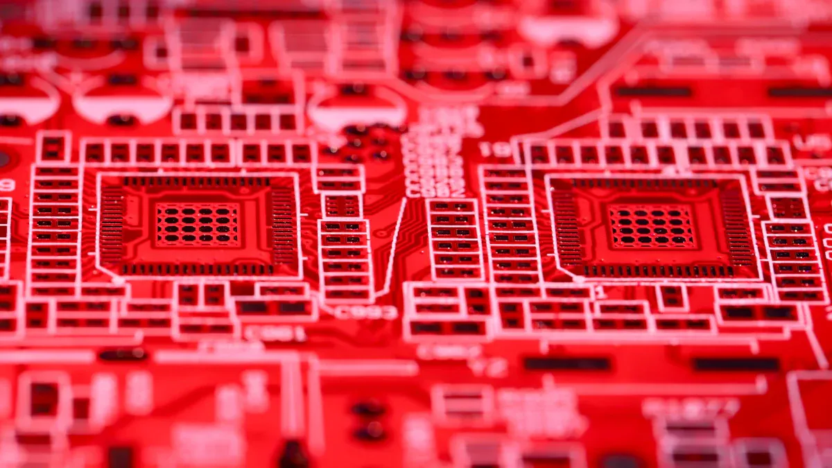
Integrated Circuit Packaging: Technologies, Standards, and Future Trends
Integrated circuit packaging helps decide how semiconductors will work in the future. Engineers use packaging to make semiconductors work better. It also helps make devices smaller and faster.
Integrated circuit packaging helps decide how semiconductors will work in the future. Engineers use packaging to make semiconductors work better. It also helps make devices smaller and faster. The industry started with simple integrated circuit packaging. Now, it uses advanced solutions for more complex systems. These solutions also help with mixing different types of parts. Packaging is now very important for making semiconductors better. People who watch packaging changes can help create new ideas.
Key Takeaways
-
Integrated circuit packaging keeps chips safe. It connects different parts together. It also helps devices get smaller and faster. This makes them work better and last longer.
-
Advanced packaging methods like 3D stacking, fan-out wafer-level packaging, and chiplet designs make things work better. They use less power. They also help build more complex systems.
-
Industry standards from JEDEC and IPC make sure packaging and testing are good. They help keep things safe and make sure parts work together.
-
New materials and cooling technologies help control heat. They also make modern semiconductor packages last longer.
-
Companies work together and keep inventing new things. This helps solve problems in making chips. It also helps improve packaging in the future.
Integrated Circuit Packaging Overview
Purpose and Functions
Integrated circuit packaging is very important for how well electronics work. Engineers use ic packaging to put chips and other parts together. This makes a full system. It helps make things smaller and lets them work faster. Smaller parts like 0201 and 01005 show how ic packaging shrinks devices but adds more features.
Some main jobs of ic packaging are:
-
Giving support to circuits and other parts
-
Making electrical paths for fast signals and data
-
Handling heat with cooling tools like micro heatpipes
-
Keeping the ic safe from damage and the environment
-
Helping stack parts in 3D with System on Package and Package on Package
-
Making things last longer with strong tests and new materials
Engineers look for new materials, like carbon nanotubes, to make ic packaging better. The substrate in ic packaging is also key for making things smaller and work better.
Evolution of IC Packaging
The story of ic packaging shows how fast semiconductors have changed. In the 1970s, multi-chip modules started mixing different parts. Old ic packaging ways changed into new ones that put logic, memory, sensors, and antennas together. Moore’s Law could not keep up with just 2D, so the industry moved to 3D stacking and mixing parts.
New ideas like through-silicon vias, interposers, and fan-out wafer-level packaging changed ic packaging. These let devices work better, get smaller, and do more. Now, device, package, and PCB design work together for custom solutions in high-speed computing and IoT. This change shows how integrated circuit packaging went from simple boxes to complex systems with many technologies.
Industry Snapshot:
Key Statistic
Details
Market Size (2024)
Projected Market Size (2033)
USD 90.18 billion
CAGR (2025-2033)
9.35%
Largest Regional Market
Asia-Pacific
Fastest Growing Region
North America
Dominant Type Segment
Organic substrates
Dominant End-User Segment
Consumer electronics
Key Packaging Technologies
SOP, DFN, GA, FOWLP
Market Drivers
Demand for consumer electronics, 5G, packaging innovations
Major Market Players
Amkor, ASE Group, Henkel, Hitachi Chemical, Sumitomo Bakelite, LG Chem, Powertech, Toray
Notable Trends
Adoption of FOWLP for performance and miniaturization
Regional Highlights
China’s industry grew 18.5% in 2023; US leads North America with 75% share
Strategic Factors
R&D, collaborations, government initiatives
IC Packaging Technologies
Traditional Packages
Engineers have used traditional ic packaging for many years. These packages help protect and connect chips. Some common types are Dual In-line Package (DIP), Plastic Leaded Chip Carrier (PLCC), and Quad Flat Package (QFP). Each type works best for certain devices.
-
DIP has two rows of pins. It can have 8 to 42 pins. The pins are spaced from 1.778 to 2.54 mm apart. DIP is good for through-hole mounting. Ceramic DIPs are very reliable.
-
PLCC has J-shaped leads. It can have 20 to 84 pins. PLCC saves space and can be mounted on surfaces or in sockets.
-
QFP has gull-wing leads. It can have 32 to 240 pins. The pin spacing can be as small as 0.4 mm. QFP has exposed pads to help with heat.
These traditional ic packaging types are mature and cost less. They work well for many uses. But they have limits in pin count, size, and how well they perform. As devices get smaller and more complex, engineers need new ways to package chips.
Note: Traditional ic packaging uses longer connections. This can cause more signal loss and lower density.
|
Package Type |
Pin Count Range |
Pitch Range (mm) |
Body Dimensions (mm) |
Thickness Range (mm) |
Key Performance Highlights |
|---|---|---|---|---|---|
|
DIP |
8 - 42 |
1.778 - 2.54 |
Width: 6.35 - 13.97 |
0.81 - 12.96 |
Mature, inexpensive, through-hole mounting, ceramic versions for high reliability |
|
PLCC |
20 - 84 |
1.27 |
Width/Length: 9 - 29.28 |
3.56 - 4.57 |
J-leads, surface or socket mount, space-efficient lead shape |
|
QFP |
32 - 240 |
0.4 - 0.8 |
Width/Length: 5 - 45.7 |
1 - 4.9 |
Gull-wing leads, surface mount, ceramic versions for high reliability, exposed pads for heat sinking |
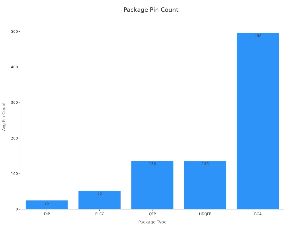
Advanced Solutions
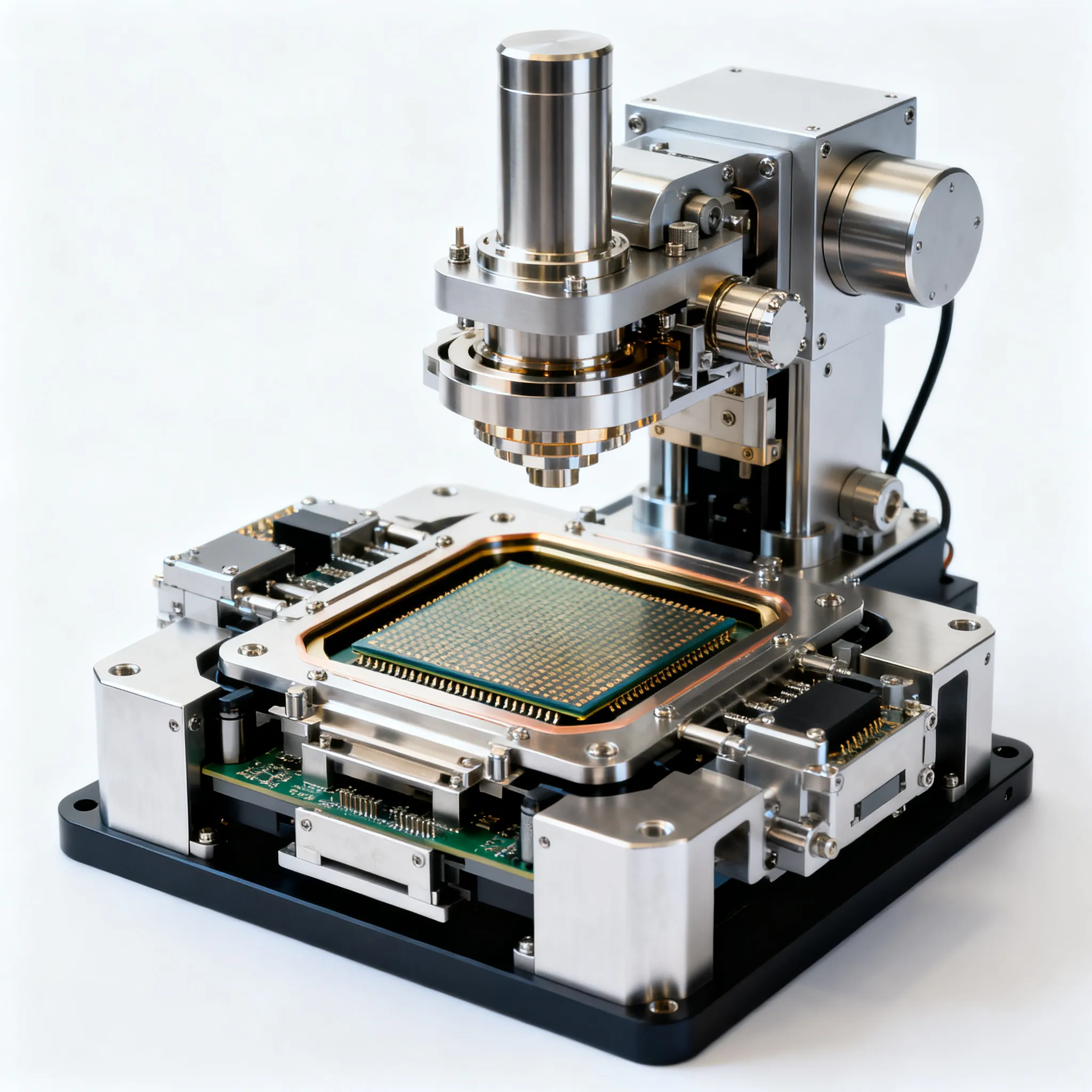
Advanced packaging has changed how engineers design ic packaging. These new ways include Ball Grid Array (BGA), Chip Scale Package (CSP), Wafer-Level Package (WLP), Fan-Out Wafer-Level Package (FOWLP), and system-in-package (SiP). These help make connections shorter, add more pins, and improve signals.
-
BGA uses solder balls instead of leads. It can have up to 975 pins. BGA gives better heat and electrical performance.
-
CSP and WLP make the package almost as small as the chip. This helps make devices even smaller.
-
FOWLP lets more parts fit in one package. It also helps with heat.
-
SiP puts different ic types, like logic, memory, and RF, together. This helps make complex devices.
Engineers use these advanced ways for fast data, small size, and better heat control. These methods also cut down on interference and make devices more reliable. Flip chip bonding and through-silicon vias (TSVs) make tiny connections. These features help signals and reduce unwanted effects.
-
In smartphones, advanced ic packaging puts processors, memory, and RF modules together. This makes phones powerful and small.
-
In cars, strong SiP modules help electronics work in tough places.
-
In data centers, fast processors use advanced packaging for better speed and less power.
Tip: Advanced ic packaging lets chips stack up and use shorter connections. This means faster speeds, less delay, and better performance.
3D IC Packaging
3D ic packaging is a big step in chip technology. This method stacks ic layers on top of each other. It uses things like through-silicon vias and silicon interposers. Engineers use 3D ic packaging for higher density, better signals, and less power use.
-
In 2024, over 42 billion 3D-stacked die units shipped. This shows many people use 3D ic packaging now.
-
3D packages can have up to 2,300 connections per cm².
-
FOWLP has thermal resistance as low as 0.6 °C/W. This helps with heat.
-
3D-stacked packaging now makes up 28% of logic chip revenue.
|
Metric / Trend |
Value / Statistic |
Description |
|---|---|---|
|
3D-stacked die units shipped (2024) |
Over 42 billion |
Rapid adoption of 3D IC packaging |
|
Interconnect density in 3D packages |
2,300 I/Os per cm² |
Increased integration density |
|
Thermal resistance in FOWLP |
0.6 °C/W |
Improved thermal performance |
|
3D-stacked packaging revenue share |
28% of total logic chip revenue |
Significant market contribution |
|
AI accelerators using advanced packaging |
Over 72% (2024) |
High adoption in performance segments |
|
Signal integrity improvement (FO-PLP) |
30% better than FO-WLP |
Enhanced signal quality |
|
Parasitic inductance reduction |
24% decrease |
Electrical performance gains |
|
TSV resistance improvement |
19% better |
Advances in vertical interconnect technology |
|
Power savings via chiplet packaging |
18% average savings |
Energy efficiency gains |
|
Die stacking levels in commercial DRAM |
Up to 8 layers |
Advancement in vertical integration |
Engineers use chiplet designs to build complex systems with small, reusable blocks. Chiplet packaging lets them mix different functions, like logic, memory, and analog, in one SiP. This helps third-party chiplet designs and makes products faster to develop.
-
Chiplet packaging makes connections shorter and signals better.
-
Embedded die technology cuts delay by 22% and saves up to 18% power.
-
Flip chip bump pitch is now about 80 µm in sub-5nm designs. This helps make things smaller.
Note: The advanced packaging market was $70.3 billion in 2024. It grew by 13.2% each year. By 2026, over 40% of processor gains will come from ic packaging improvements.
Engineers use SiP and chiplet solutions for new devices. These ways help make devices smaller, faster, and cheaper. As the industry grows, ic packaging will be even more important for better performance and new ideas.
Industry Standards
JEDEC and IPC
JEDEC and IPC make important rules for integrated circuit packaging. These groups write documents to help companies design and test products. JEDEC makes rules for semiconductor devices. IPC makes rules for printed circuit boards and assemblies. They work together to keep products safe and high quality.
|
Standard / Document Title |
Standard Number |
Date |
Purpose |
Committee(s) |
|---|---|---|---|---|
|
Moisture/Reflow Sensitivity Classification for Non-hermetic SMDs |
J-STD-020F |
Dec 2022 |
Defines moisture sensitivity levels for safe packaging and handling |
JC-14, JC-14.1 |
|
Handling, Packing, Shipping, and Use of Moisture/Reflow Sensitive SMDs |
J-STD-033D |
Apr 2018 |
Standardizes handling and shipping to prevent damage |
JC-14, JC-14.1 |
|
Preconditioning of Nonhermetic Surface Mount Devices Prior to Reliability Testing |
JESD22-A113I |
Apr 2020 |
Sets preconditioning flow for reliability testing |
JC-14.1 |
|
Package Warpage Measurement of Surface-Mount ICs at Elevated Temperature |
JESD22-B112C |
Nov 2023 |
Measures package warpage during soldering |
JC-14, JC-14.1 |
|
Adapter Test Board Reliability Test Guidelines |
JEP176A |
Jun 2025 |
Guides reliability tests for ICs with adapter boards |
JC-14, JC-14.3 |
These rules help companies make fewer mistakes and work better together. They also help companies follow laws for medical, car, and home electronics.
Quality and Interoperability
Quality and interoperability are very important for integrated circuit packaging. IPC rules like IPC-A-600 and IPC-6012 set clear steps for good looks and performance. The table below shows some main IPC rules and what they do:
|
IPC Standard |
Focus Area |
Role in Validating Reliability of IC Packaging Technology |
|---|---|---|
|
IPC-A-600 |
Visual acceptability of printed boards |
Ensures only defect-free PCBs pass inspection, supporting packaging reliability. |
|
IPC-6012 |
Qualification and performance of rigid PCBs |
Defines requirements for durability and long-term reliability. |
|
IPC-A-610 |
Acceptability of electronic assemblies |
Guides assembly quality, soldering, and component placement. |
|
IPC-2221 |
Generic standard on PCB design |
Establishes best practices to reduce errors and improve consistency. |
|
IPC-7711/7721 |
Rework, modification, and repair |
Offers safe rework and repair processes, maintaining quality after modifications. |
Testing is important for making sure products work well together:
-
Built-in self-test algorithms find problems in fast connections.
-
Signal Integrity Monitors check the health of chip links.
-
Redundancy and repair use extra lanes to keep signals strong.
-
High-Speed Access and Test features help test chips at every step.
-
Environmental testing checks how chips work with changes in heat, power, and process.
Companies use these rules and tests to make sure their products are strong and work well for important jobs.
Trends in IC Packaging
3D Integration
3D integration is a big trend in ic packaging. This method stacks many ic layers on top of each other. They connect the layers with special links called through-silicon vias. Companies use 3D stacking to make devices work better and use less power. It also helps make devices smaller. The industry checks progress with key numbers like package, performance, power, profile, cost, and cycle time. Doug Yu from TSMC made these numbers to help guide new ideas.
|
Aspect |
Details |
|---|---|
|
Key Performance Indicators (KPIs) |
Package, Performance, Power, Profile, Cost, Cycle Time (PPPCC) |
|
Adoption Challenges |
TSV technology not widely adopted in cost-sensitive mobile applications due to cost and technical issues |
|
Closure of Quimonda in 2008 delayed DRAM stacking adoption |
|
|
Competition from fan-out wafer-level packaging (FOWLP) displaced some 3D IC adoption |
|
|
Adoption Examples |
Some smartphones use TSV-based 3D ICs, indicating volume production |
|
Milestones |
SK Hynix introduced 3D TSV DRAM stacks (HBM) in 2015 |
|
3D system integration via wafer-to-wafer (W2W) and die-to-wafer (D2W) stacking expected around 2022 |
|
|
Future Developments |
Hybrid bonding and pitch scaling to improve yield and performance in D2W stacking |
|
Industry roadmap and expert consensus support ongoing 3D integration advancements |
Engineers keep working to fix cost and technical problems in 3D integration. Hybrid bonding and pitch scaling can help make more chips and boost performance. Many smartphones now use 3D ic packaging, so this trend is now common. Experts think 3D integration will keep growing as new chip designs appear.
Fan-Out and Wafer-Level
Fan-out wafer-level packaging and wafer-level chip scale packaging have changed ic packaging a lot. These new types help make devices smaller and pack in more parts. The market for wafer-level chip scale packaging was almost $4.9 billion in 2023. It could grow to over $37 billion by 2031. This fast growth shows many companies are using these new ways.
-
Fan-in WLCSP lets devices be smaller and cheaper with more parts.
-
Fan-out wafer-level packaging adds more I/O by spreading wires outside the chip. This helps with heat and lets more parts fit.
-
Better pitch technology and new materials help make more good chips and lower costs.
-
Shorter links and better heat control make devices work better and last longer.
📈 Industry Insight:
Fan-out wafer-level packaging and wafer-level chip scale packaging help make devices smaller and improve chip yields. These ways let companies make smaller, stronger devices for less money.
Engineers use these packaging types for phones, wearables, and car electronics. The push for smaller, better devices keeps driving new ic packaging ideas.
Heterogeneous Integration
Heterogeneous integration is now a main trend in ic packaging. This way puts different ic types, materials, and jobs in one package. Engineers use through-silicon vias to link many chips on a substrate. This breaks old size limits. It also helps make systems cheaper and lets chiplet-based systems work.
New 3D heterogeneous integration lets chips connect at very small sizes, even down to submicron. The industry now uses 3D stacking, mixing many jobs, and hybrid integration. These changes bring high density, lower power use, smaller size, and better reliability.
Chiplet designs are very important for this trend. Designers can pick chiplets for logic, memory, or analog jobs. This makes system-in-package solutions flexible and fast to build. It also helps new products come out faster and supports new ideas in chips.
💡 Tip:
Heterogeneous integration and chiplet designs help engineers make complex systems faster and easier. This trend meets the need for small, powerful electronics.
Advanced Materials
Advanced materials are behind many new trends in ic packaging. Engineers pick materials that move heat well, work better with electricity, and last longer. These materials help with high-power ic needs. Copper links, low-k dielectrics, and new substrates make new packaging types possible, like 3D packaging and wafer-level packaging.
-
New cooling materials, like microfluidic cooling and built-in heat pipes, help keep chips cool and last longer.
-
Better thermal interface materials help chips handle more heat.
-
Heterogeneous integration uses many semiconductor materials in one package. This boosts performance and cuts power use.
-
The industry is making recyclable and green packaging to help the planet.
-
Packaging must handle heat, power, temperature changes, and signal problems like EMI and crosstalk.
-
Smaller devices need tiny, complex packages that still work well and cost less.
Engineers keep looking for new materials to help new technologies and chip designs. These efforts make sure ic packaging keeps up with what modern chips need.
🔍 Note:
The move to advanced materials and new packaging ways will shape the future of ic packaging. Companies that work on these areas will lead the next big changes in chips.
Challenges and Considerations
Manufacturing Complexity
Integrated circuit packaging has many problems in making products. The industry must follow many steps and strict rules. Studies show some big problems in making these products:
-
Not enough semiconductor factories means fewer chips get made. This slows down new technology.
-
Relying on parts from other countries can cause supply chain problems.
-
Hard government rules make it tough to build new factories. This slows down the market.
These things make it harder to make more packaging. Companies need to buy better machines and hire skilled workers. Cleanrooms and special tools are needed for this work. As packaging gets better, every step must meet higher standards.
Testing and Reliability
Testing and reliability are very important in packaging. Companies use new quality control systems to get better results. For example:
-
A company in Taiwan tested a new real-time quality control system.
-
The system uses special methods to find the best settings.
-
This helps make better products and fewer mistakes.
-
Quality checks look at how well circuit probe tests work.
-
The system helps smart factories keep high standards before packaging.
These ways help companies find problems early and make sure products work well. As chips get smaller, testing must be even more careful.
Cost and Scalability
Cost and scalability are big worries in packaging. New packaging needs costly materials and machines. Companies must try new things but also keep prices low. Making more products can use up money and resources. Small companies may have trouble competing with bigger ones. The industry looks for ways to save money but still make good products and meet demand.
Ecosystem Collaboration
Ecosystem collaboration helps packaging move forward. One company cannot do everything alone. Working together with suppliers and equipment makers helps create new ideas. Sharing rules and talking openly makes it easier to fix problems and work faster. Teamwork also helps with supply chain problems and keeps parts coming.
💡 Good teamwork in the ecosystem brings faster progress and better packaging solutions.
Integrated circuit packaging is still very important for semiconductors. The table below shows how packaging helps the industry grow and change:
|
Metric / Trend |
Details |
|---|---|
|
~$697 billion |
|
|
Market Growth Rate (2025-2030) |
7%–9% annually |
|
Key Technologies |
3D stacking, system-in-package, fan-out wafer-level packaging |
People who watch packaging trends can keep up with new needs. They can also help lead new technology. Packaging will stay important for better performance and new uses in the future.
FAQ
What is integrated circuit packaging and why is it important?
Integrated circuit packaging keeps chips safe from harm. It connects chips to other parts in a device. It also helps move heat away from the chip. This makes devices work better and last longer. Engineers use packaging to make electronics stronger and faster.
How do advanced packaging technologies improve semiconductor performance?
Advanced packaging technologies make connections shorter. This helps signals move faster and better. These ways let more parts fit in a small space. Devices can run quicker and use less power. This makes electronics work well and saves energy.
What are chiplet-based designs and why are they popular?
Chiplet-based designs use small blocks called chiplets. Engineers can mix different chiplets in one package. This helps make new devices faster. Chiplet designs let companies use parts from others. Universal chiplet interconnect express helps link chiplets together.
Which standards guide ic packaging and manufacturing processes?
JEDEC and IPC make rules for ic packaging and testing. These rules help companies make good and safe products. They also help different companies work together. The rules support new ways to make and test ic packaging.
What trends are shaping the future of ic packaging?
Trends include 3d stacking, chiplet systems, and new materials. Engineers use these to make smaller and faster devices. The industry also works on green packaging to help the planet. New ideas help electronics work better and last longer.