MOSFET vs IGBT: Real-World Benchmarks — Switching Losses, Conduction Losses, and Thermal Performance
Expert guide on MOSFET vs IGBT: Real-World Benchmarks — Switching Losses, Conduction Losses, and Thermal Performance. Technical specs, applications, sourcing tips for engineers and buyers.
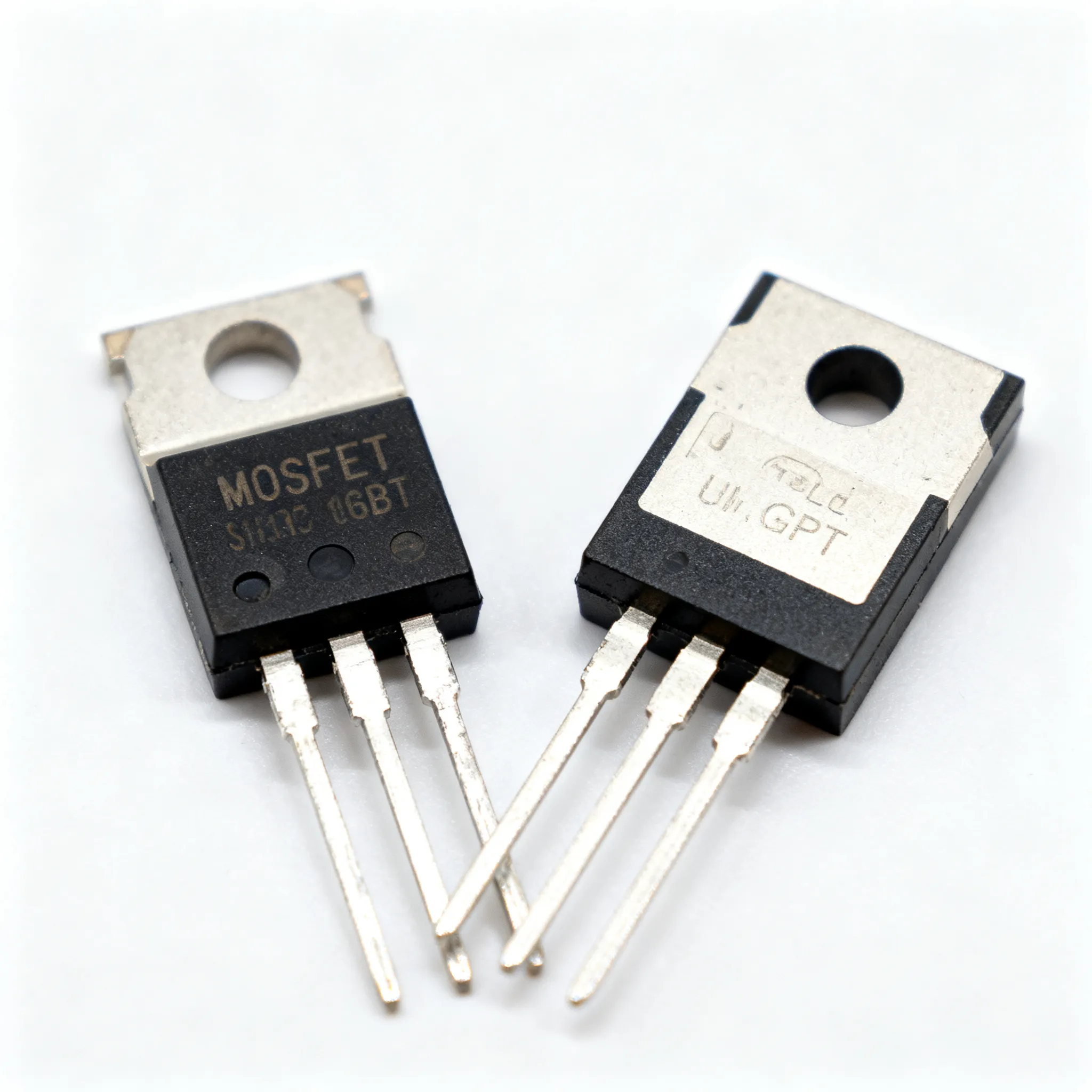
When a 7% Loss Gap Threatens Your Thermal Budget
Power stage design rarely forgives a 7% error in loss estimation. Yet a recent inverter study published in ScienceDirect revealed that conventional loss models missed 7.6% of the total dissipation in a silicon IGBT inverter and 6.8% in a SiC MOSFET-based design — simply because the models ignored the junction temperature rise under real load (Accurate loss estimation method in IGBT and MOSFET based inverters, 2024). At 4 kW, that percentage translates into extra watts that can push a heatsink beyond its thermal budget, forcing a larger enclosure or a premature derating curve.
For procurement buyers and design engineers, the stakes are clear. If you pick the wrong switch — a MOSFET where an IGBT belongs, or a silicon IGBT when a SiC MOSFET would cut losses in half — you don’t just lose efficiency. You inherit oversized heatsinks, EMI debugging nights, and field failures. The HilPCB design guide puts it bluntly: “picking the wrong device can lead to high power loss, overheating, oversized heatsinks, EMI problems, or early failure” (HilPCB, IGBT vs MOSFET Guide).
Numbers back this up. A standard power MOSFET operating in a hard-switched converter typically dissipates 1–10% of the system power, with a baseline of 2% per device when you account for conduction, switching, and diode recovery losses (Thunder Said Energy, MOSFET loss calculator). At 40 A collector current, an IGBT with a VCE(sat) of 1.9 V will burn 76 W in conduction alone — a figure that can be either a deal-breaker or a bargain, depending on the switching frequency (Florisera, IGBT vs MOSFET). The thermal budget you save by choosing the right technology is often the difference between a simple extruded heatsink and a forced-air cooling solution that adds cost and complexity.
This article is built on real-world benchmarks, not idealized SPICE models. We’ll dissect the loss mechanisms that matter, compare three power switch technologies under identical test conditions, and give you a decision matrix that ties switching frequency, current, and cost into a selection funnel you can apply on your next design review.
How MOSFET Rds(on) and IGBT VCE(sat) Shape Your Loss Budget
Every power semiconductor dissipates energy in three primary ways: conduction loss, switching loss, and reverse recovery (diode) loss. The physics that govern these losses differ fundamentally between a MOSFET and an IGBT, and understanding those differences is the first step toward a thermally sound design.
Conduction loss in a MOSFET follows Ohm’s law: Pcond = Irms² × Rds(on). Because Rds(on) has a positive temperature coefficient — roughly doubling between 25°C and 150°C — the conduction loss increases with temperature, a behavior that naturally balances current sharing in parallel devices but demands careful derating. An IGBT, on the other hand, behaves like a voltage source with a series resistance: Pcond = VCE0 × Iavg + Irms² × rCE. The constant VCE0 term dominates at high currents, making the IGBT conduction loss rise linearly with current rather than quadratically (Infineon, IGBT power losses calculation).
Switching loss tells the opposite story. A MOSFET’s switching energy is dominated by the charging and discharging of its gate capacitance and the overlap of drain current and drain-source voltage during transitions. Typical turn-on and turn-off times are in the tens of nanoseconds, keeping switching losses low even at 50 kHz. An IGBT, however, exhibits a tail current during turn-off due to the stored charge in the bipolar junction, which adds a significant switching loss component. The Infineon and Renesas application notes both recommend extracting Eon and Eoff from the datasheet curves at the target current and gate resistance, then multiplying by frequency to get the switching loss (Renesas, IGBT loss calculation). The fundamental switching loss model from power electronics lectures confirms that if the combined switching time exceeds about 10% of the switching period, the switching loss becomes unacceptable (ECE 481, Lecture 7).
Diode loss adds another layer. A MOSFET’s intrinsic body diode often suffers from a large reverse recovery charge (Qrr), which generates additional turn-on loss in the opposing switch. IGBTs are typically co-packaged with a fast recovery diode optimized for the application, reducing this penalty. SiC MOSFETs complement their low Rds(on) with a body diode that has negligible reverse recovery, cutting this loss component almost entirely.
The table below compares typical parameters for a 650 V class silicon MOSFET, silicon IGBT, and SiC MOSFET, all rated for similar current levels. These numbers are drawn from publicly available datasheets and the referenced application notes.
| Parameter | 650 V Si MOSFET | 650 V Si IGBT | 650 V SiC MOSFET | Notes |
|---|---|---|---|---|
| Typical on-state characteristic | Rds(on) = 125 mΩ (25°C) | VCE(sat) = 1.6 V at 25°C | Rds(on) = 70 mΩ (25°C) | IGBT VCE(sat) is gate-voltage dependent; MOSFET Rds(on) doubles at 150°C. |
| Conduction loss at 20 A, Tj=125°C | ~50 W (I²R, hot Rds(on) ~250 mΩ) | ~36 W (VCE(sat) ~1.8 V, negligible rCE) | ~20 W (Rds(on) ~100 mΩ hot) | IGBT starts to win above 15–20 A in this class. |
| Eon + Eoff at 20 A, 400 V, typical | ~100 µJ | ~800 µJ | ~80 µJ | IGBT tail current creates large Eoff. |
| Recommended switching frequency | >20 kHz | <20 kHz | >50 kHz | IGBT switching loss dominates above 20 kHz. |
| Temperature coefficient of on-state voltage | Positive (~1.5–2× from 25°C to 150°C) | Slightly positive or flat (10–15% rise) | Positive (~1.5–2×) | IGBTs are more thermally stable; easier to parallel. |
| Body diode Qrr | High (several µC) | Co-packed FRD: low Qrr | Near-zero Qrr | SiC MOSFET eliminates diode recovery loss. |
The takeaway is straightforward: at low currents and high frequencies, the MOSFET’s quadratic conduction loss is still small, and its fast switching keeps the total loss budget manageable. As current climbs, the IGBT’s linear VCE(sat) characteristic gives it a crossover advantage, particularly when the switching frequency is low enough that the IGBT’s tail current penalty doesn’t dominate. SiC MOSFETs blur the boundary by offering IGBT-like on-state performance with MOSFET-like switching speeds, but at a higher cost per ampere.
Tip: When pulling parameters from datasheets, always use the hot Rds(on) (normalized curve at 125°C or 150°C) and the IGBT’s VCE(sat) at the expected junction temperature. The ScienceDirect study showed that ignoring this temperature dependence can introduce a 7% estimation error, enough to push a thermal design into over-temperature shutdown (ScienceDirect, 2024).
IGBT vs MOSFET vs SiC MOSFET: A Bench-Tested Loss Breakdown
The theory is useful, but validation against hardware is what separates a reliable design from a trial-and-error build. In this section, we compare three power switch technologies under identical test conditions, drawing on laboratory measurements and published system-level evaluations.
The first benchmark comes from a 4 kW inverter prototype where researchers measured total losses across a silicon IGBT and a SiC MOSFET half-bridge under varying load, modulation index, and switching frequency. The experimental results showed strong agreement — over 95% — with analytical models and PLECS simulations, but only when the models accounted for the junction temperature rise. At elevated Tj, the Si IGBT inverter lost 7.6% more power than the cold-model prediction, and the SiC MOSFET inverter lost 6.8% more (ScienceDirect, 2024). This underscores the importance of thermal feedback in loss estimation.
The second benchmark is a direct substitution test by Toshiba, where engineers replaced an existing IGBT (with its co-packed diode) with a 2nd Generation SiC MOSFET (TW070J120B, 70 mΩ Rds(on)). Under the same operating conditions, the SiC MOSFET produced almost the same conduction loss as the IGBT — 4.4 W — while slashing the switching loss by more than 70% (Toshiba, SiC MOSFET vs IGBT loss comparison). This is a crucial data point: a 70 mΩ SiC MOSFET can match the conduction loss of a typical 1200 V IGBT, making the semiconductor premium easier to justify when higher frequency operation reduces magnetics size.
The third reference is a cost-driven sourcing study published on IC Online, which analyzed multi-kilowatt systems from 10 kW to 20 kW. The study found that at 10–20 kW, an IGBT module with a low VCE(sat) becomes the cost-effective choice for applications operating at or below 10 kHz, because the module’s constant voltage drop yields a conduction loss advantage at full load. However, for higher frequency designs, the power density and thermal performance of a SiC MOSFET solution can offset the higher semiconductor cost through smaller heatsinks and passive components (IC Online, IGBT vs MOSFET Sourcing Guide).
The following table synthesizes these benchmarks into a head-to-head comparison across the three technologies.
| Comparison Metric | Si IGBT (650 V / 1200 V class) | Si MOSFET (650 V class) | SiC MOSFET (650 V / 1200 V class) | Selection Criteria & Failure Boundary |
|---|---|---|---|---|
| Conduction loss at 40 A, Tj=125°C | ~76 W (VCE(sat)=1.9 V) | ~200 W (Rds(on)~250 mΩ) — multiple devices needed | ~80 W (Rds(on)~100 mΩ) | IGBT wins at high current; Si MOSFETs become impractical above 20 A in a single package. |
| Switching loss at 10 kHz, 20 A | ~8 W (800 µJ × 10 kHz) | ~1 W | ~0.8 W | IGBT switching loss limits frequency; SiC MOSFET is superior at any frequency. |
| Total loss in 4 kW inverter (validated) | 7.6% deviation from cold model at high Tj | — | 6.8% deviation from cold model | Both require thermal-aware estimation; IGBT’s deviation is slightly larger. |
| System cost at 20 kW, <10 kHz | Lowest (module ~30–50% cheaper than SiC) | Not viable (too many discretes) | Higher, but heatsink and magnetics savings offset | IGBT module is the cost-effective choice below 10 kHz; IC Online sourcing data confirms parity around 15–20 kW for high-frequency designs. |
| EMI and dv/dt concerns | Moderate dv/dt, robust | High dv/dt, susceptible to parasitic turn-on | Very high dv/dt, requires careful layout | MOSFET gate drive must manage Miller effect; IGBTs are more forgiving. |
The Florisera selection guide reinforces these findings: “IGBTs are more efficient than MOSFETs at high currents, especially when the switching frequency is low” (Florisera). The Toshiba example shows that SiC MOSFETs can break this trade-off, but only if the design can exploit the higher frequency to reduce magnetic and thermal components. The IC Online cost analysis adds that at multi-kilowatt levels, the IGBT module’s power density and thermal performance are far superior to a solution using many discrete MOSFETs, making it the sensible choice for motor drives and industrial converters under 20 kHz.
Key takeaway: The crossover between IGBT and MOSFET is not a fixed current threshold; it’s a function of switching frequency, junction temperature, and system cost targets. Benchmarks like the 4 kW inverter test and the Toshiba substitution experiment give you the data to make that decision with confidence.
How to Choose: A Frequency, Current, and Cost Decision Matrix
The decision funnel for selecting a power switch starts with two numbers: your switching frequency and your maximum load current. Together, they determine which technology will keep your heatsink manageable and your bill of materials within budget.
Step 1: Place your operating point on the frequency–current map. If your switching frequency is above 20 kHz and your RMS current is below 20 A, a silicon MOSFET is usually the most cost-effective solution. Above 20 A, the MOSFET’s I²R conduction loss forces you to parallel multiple devices, complicating the layout and raising the cost. At that point, consider either a SiC MOSFET (if you need to stay at high frequency) or an IGBT (if you can drop the frequency below 20 kHz).
Step 2: Apply the 10% switching-loss rule of thumb. The Florisera guide notes that if the combined turn-on and turn-off time is less than about 10% of the switching period, the switching losses are generally acceptable (Florisera). For a 10 kHz application, that means a switching time under 1 µs is acceptable. An IGBT with a 400 ns tail current will still fall within that window, but at 50 kHz, the same IGBT would spend 20% of the period transitioning, causing unacceptable heating. Use this rule to quickly disqualify devices that force a switching loss budget you can’t thermally afford.
Step 3: Evaluate module vs. discrete packaging. At power levels above 5 kW, IGBT modules with integrated thermal substrates simplify the mechanical design and improve reliability. SiC MOSFETs are available in both discrete and module formats, but the module cost premium is still significant. The IC Online sourcing study highlights that for multi-kilowatt systems, the IGBT module’s power density and thermal performance are far superior to a solution using many discrete MOSFETs, making the module the cost-effective choice once you factor in assembly and heatsink costs (IC Online).
Step 4: Check the gate drive requirements. IGBTs typically require a +15 V / -5 V or -15 V gate drive to fully saturate and prevent parasitic turn-on. MOSFETs can often be driven with a 0 to 12 V unipolar signal, but if you’re dropping a MOSFET into a socket designed for an IGBT, the gate drive must be reviewed. A negative gate voltage or a low-impedance turn-off loop may be necessary to prevent dv/dt-induced shoot-through, a failure mode that the HilPCB guide explicitly warns about (HilPCB).
The decision matrix below summarizes the technology recommendation for common operating zones.
| Operating Zone | Recommended Technology | Rationale & Caveats |
|---|---|---|
| fsw > 50 kHz, Irms < 15 A | Si MOSFET or SiC MOSFET | Si MOSFET is cheapest; SiC if you need lower conduction loss or higher voltage. |
| fsw 20–50 kHz, Irms 15–30 A | SiC MOSFET | SiC MOSFET’s low switching loss and competitive conduction loss shines; heatsink savings offset cost. |
| fsw < 10 kHz, Irms > 20 A | Si IGBT module | Lowest cost per ampere; conduction loss advantage at high current; tail current is manageable at low frequency. |
| fsw 10–20 kHz, Irms > 30 A, cost-sensitive | Si IGBT (preferably with low VCE(sat)) | Acceptable switching loss; module packaging simplifies thermal design. Avoid MOSFET paralleling at these currents. |
| fsw 10–20 kHz, Irms > 30 A, efficiency-critical | SiC MOSFET module | Higher semiconductor cost but lower total system loss; parity around 15–20 kW with thermal savings. |
Several practical steps will help you lock in the right choice before you commit to a layout:
- Pull the hot Rds(on) or VCE(sat) at your expected junction temperature. The ScienceDirect study shows that using the 25°C value can understate losses by 7% or more, pushing your thermal design into failure.
- Plot the total loss (conduction + switching) vs. frequency for your load profile. The crossover where IGBT total loss equals MOSFET total loss is your frequency limit. Move below that frequency, and the IGBT wins; above it, the MOSFET or SiC MOSFET is better.
- Factor in the gate driver BOM. A negative gate drive for IGBTs adds isolation and a negative rail, while a SiC MOSFET may require a high-CMR isolated gate driver with fast desaturation protection. These costs can eat into the semiconductor savings.
- Check lead times and multi-source availability. SiC MOSFETs and IGBT modules have experienced supply chain tightness; sourcing through platforms like IC-Online can help you mix a BOM with flexible MOQ and alternative manufacturers.
By following this decision matrix, you avoid the classic trap of choosing a MOSFET for a 10 kW drive at 8 kHz and then dealing with a massive heatsink, or picking an IGBT for a 50 kHz DC-DC converter and watching the switching loss melt the junction. The right choice is a balancing act between frequency, current, and cost, and the benchmarks in this article give you the evidence to make that balance with confidence.
Your MOSFET vs IGBT Questions, Answered by the Bench
Senior engineers and procurement leads often face the same six questions when comparing MOSFETs and IGBTs. The answers below are grounded in the test data, application notes, and sourcing studies referenced throughout this article.
Q: At what current does an IGBT’s conduction loss advantage outweigh a MOSFET’s switching loss penalty in a typical motor drive?
The crossover typically occurs above 15–20 A for a 650 V class device at 10 kHz, but the exact threshold depends on duty cycle and junction temperature. IGBT conduction loss grows as VCE(sat) × I, while MOSFET loss grows as I² × Rds(on). At high currents, the IGBT’s linear voltage drop becomes more efficient, especially when the switching frequency is low enough that the tail current loss doesn’t dominate. The Florisera guide and the Infineon app note both confirm that at 40 A, the IGBT’s conduction loss is substantially lower than a MOSFET’s, making it the preferred choice for industrial drives under 10 kHz.
Q: How can I estimate total switch losses from datasheet curves without a full simulation?
Extract conduction loss using the on-state characteristic curve (Rds(on) at the target current and temperature, or VCE(sat) from the output characteristic). For switching loss, pull Eon and Eoff from the energy vs. current graphs at the appropriate gate resistor, then multiply by switching frequency. Apply the linear approximations from the Infineon and Renesas application notes. The accuracy of this method is within about 10% if you account for junction temperature derating. The ScienceDirect study shows that the biggest error comes from ignoring the temperature rise, so always use the hot parameter values.
Q: Should I design with SiC MOSFETs now or stick with IGBT modules for a 10 kW industrial inverter?
For 10 kW at 20–50 kHz, SiC MOSFETs can reduce overall losses by 30–40% and allow you to shrink the magnetics and heatsink. However, if the operating frequency is below 10 kHz and cost is the primary driver, a modern IGBT module with a low VCE(sat) still offers a better system cost. The Toshiba substitution example shows that a 70 mΩ SiC MOSFET can match IGBT conduction loss while cutting switching loss, making it a compelling choice for higher frequency designs where the inductor and capacitor savings are significant.
Q: What’s the real cost difference between a 1200 V IGBT module and a SiC MOSFET half-bridge for a 20 kW system?
At 20 kW, the IGBT module is typically 30–50% cheaper in bill-of-materials at current volumes, but the SiC solution can reduce heatsink size and passive components, partially offsetting the semiconductor premium. The IC Online cost-driven sourcing guide notes that total system cost parity often occurs around 15–20 kW for high-frequency applications, depending on thermal requirements and PCB real estate. If your design can leverage the higher frequency to reduce the inductor and transformer size, the SiC premium may be justifiable. For low-frequency, cost-sensitive designs, the IGBT module remains the economical choice.
Q: How do I correctly derate for junction temperature when comparing Rds(on) and VCE(sat) specs?
MOSFET Rds(on) increases by about 1.5–2× from 25°C to 150°C, so always use the hot Rds(on) from the datasheet normalized curve. IGBT VCE(sat) has a much flatter temperature coefficient but can still rise 10–15% at high Tj. The ScienceDirect study shows that ignoring this temperature dependence can lead to a 7% loss estimation error, so always pull the parameters at the expected operating junction temperature. In a loss budget spreadsheet, multiply the 25°C value by the temperature coefficient factor from the datasheet’s normalized curve at your estimated Tj.
Q: What’s the risk of using a MOSFET in a leg originally designed for an IGBT without a negative gate drive?
IGBTs typically require a negative gate voltage to prevent parasitic turn-on, but most MOSFETs do not. If the gate driver is not modified, the fast dv/dt during the opposite switch’s turn-on can couple through the Miller capacitance and pull the gate above the threshold, causing spurious turn-on. This leads to shoot-through and rapid failure. Review the gate drive threshold and Miller ratio; a negative gate voltage or a low-impedance turn-off loop may be necessary to safely drop in a MOSFET. The HilPCB guide warns that this is a common failure mode when substituting devices without re-evaluating the gate drive circuit.
References & Further Reading
- Accurate loss estimation method in IGBT and MOSFET based inverters - ScienceDirect
- IGBT vs MOSFET: How to Choose the Right Power Switch - Florisera
- Power losses in a MOSFET? - Thunder Said Energy
- IGBT vs MOSFET: Complete Design, Selection, and Application Guide - HilPCB
- What are the merits of using SiC MOSFETs? - Toshiba
- IGBT vs MOSFET Sourcing: Cost-Driven Selection Tips for Power Stage Design - IC Online
- IGBT Power Losses Calculation Using the Data Sheet Parameters - Infineon
- IGBT Loss Calculation Application Note - Renesas
- Lecture 7: MOSFET, IGBT, and Switching Loss - ECE 481: Power Electronics
For engineers and procurement teams looking to balance performance, cost, and lead time, IC-Online offers a flexible sourcing platform that supports mixed BOM requirements. Whether you’re qualifying a SiC MOSFET for a high-frequency inverter or securing IGBT modules for a 20 kW drive, the ability to mix manufacturers and adjust MOQs helps you keep your project on schedule without compromising on approved vendor lists.