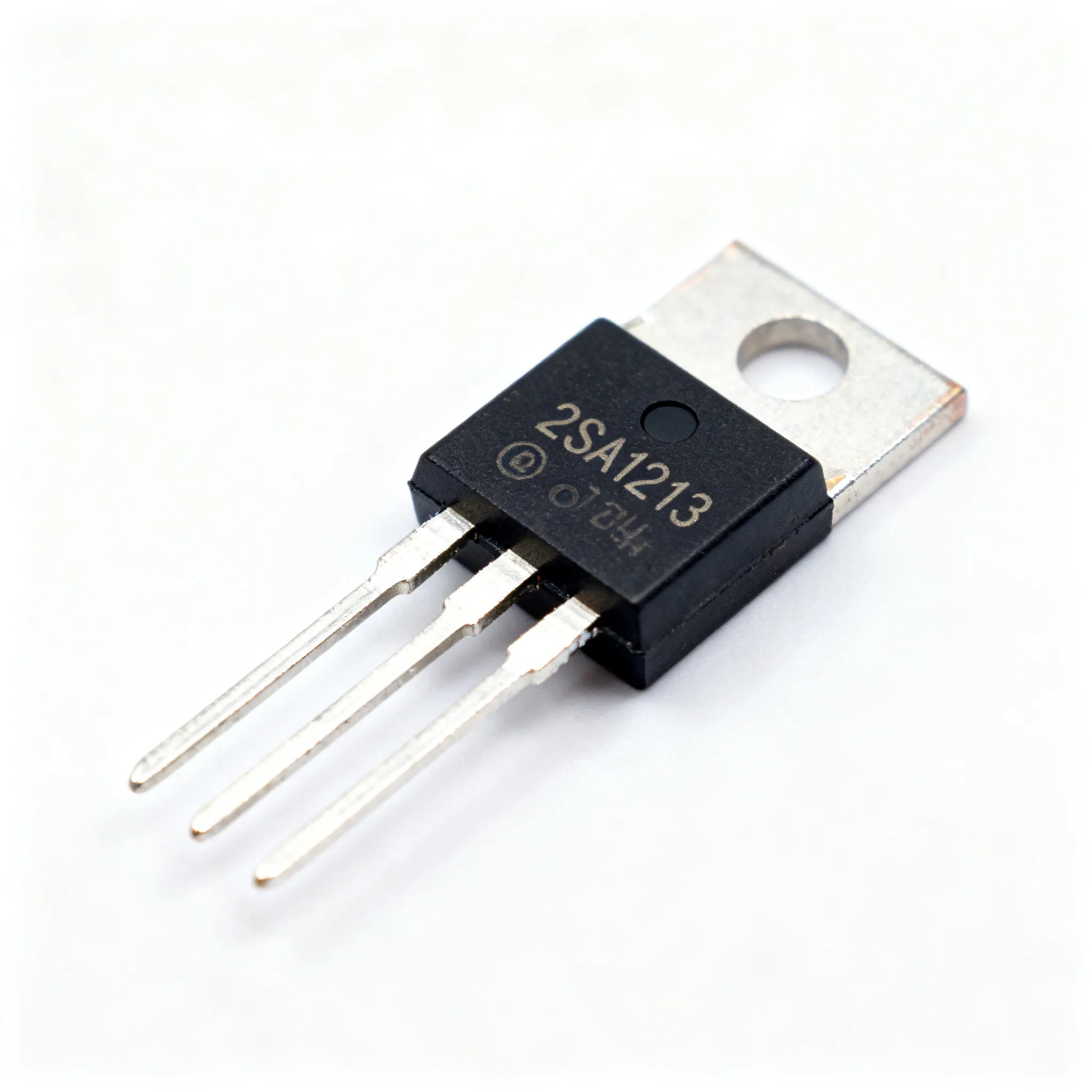
NPN and PNP Transistors and Their Impact on Circuit Design
Choosing the right transistor? NPN PNP transistors differ in polarity and speed. Their complementary pairing enables efficient circuit design for switching and amplification.

NPN PNP transistor pairs are complementary devices. They control current with opposite polarities. This enables switching, amplification, and power control in countless electronic designs.
Each type responds differently to base voltage. An npn transistor turns on when its base sits high. A pnp transistor turns on when its base pulls low.
Nova Technology Company (HK) Limited supports this field as a HiSilicon-designated (authorized) solutions partner. The company delivers chip-level solutions and system integration for semiconductor applications.
Understanding these differences gives you practical clarity. Your choice shapes amplifier behavior, logic gates, and power circuits.
Key Takeaways
- NPN transistors turn on with a high base voltage and sink current to ground.
- PNP transistors turn on with a low base voltage and source current from the positive rail.
- NPN transistors switch faster and handle current better because electrons move quicker than holes.
- Use a forced beta of 10 to 20 for base resistor sizing to keep transistors fully on.
- Choose NPN for low-side switching and PNP for high-side switching to match your load's grounding.
NPN PNP Transistor Fundamentals
Symbols, Pinouts, and Emitter Arrows
You can identify any transistor type by its schematic symbol. The emitter arrow tells you everything about how the device operates. In an npn transistor, the arrow points outward on the emitter terminal. In a pnp transistor, the arrow points inward on the emitter terminal.
| Transistor Type | Emitter Arrow Orientation |
|---|---|
| NPN | Points outward on the emitter terminal |
| PNP | Points inward on the emitter terminal |
This arrow direction shows you the path of conventional current flow. The arrow always points in the direction that conventional current moves through the emitter. For a bipolar pnp transistor, current flows into the emitter. For an NPN device, current flows out of the emitter.
Current Direction and Carrier Flow
The two types use different charge carriers. An NPN transistor relies on electrons as its majority carriers. A PNP transistor relies on holes. This difference matters because electrons move much faster through silicon than holes do.
| Material | Carrier Type | Mobility (cm²/(V·s)) |
|---|---|---|
| Crystalline silicon | Electron | 1,400 |
| Crystalline silicon | Hole | 450 |
Electron mobility in silicon reaches about 1,400 cm²/(V·s) at room temperature. Hole mobility sits near 450 cm²/(V·s). That gap explains why NPN devices switch faster and offer lower on-resistance.
PNP devices generally exhibit lower current gain and slower switching speeds due to minority carrier mobility differences in silicon substrates.
You will notice this speed difference in high-frequency analog circuits and high-speed digital designs. The higher electron mobility in NPN devices makes them the better choice for those applications. A PNP transistor still performs well in many roles, especially where you need a high-side switch or complementary pairing. The voltage you apply to the base controls both types, but the carrier physics sets their performance limits.
How PNP Transistors Work vs. NPN

Base Voltage Polarity and Turn-On
The control polarity separates these two devices more than any other trait. An npn transistor turns on when its base sits higher than its emitter. A pnp transistor turns on when its base sits lower than its emitter. You pull the base down to turn the transistor on, and you release it upward to shut it off.
The forward-bias threshold itself barely changes between the two types. Silicon needs roughly the same base-emitter voltage in both cases.
| Parameter | Silicon PNP | Silicon NPN |
|---|---|---|
| Base-emitter turn-on threshold | |V BE| ≈ 0.6–0.7 V (base pulled ~0.6–0.7 V below emitter) | V BE ≈ 0.6–0.7 V (base pulled ~0.6–0.7 V above emitter) |
| Control polarity | Turns on when base is at L level | Turns on when base is at H level |
| Current flow / role | Sources current to load (high-side switch) | Sinks current to ground (low-side switch) |
| Temperature coefficient | ≈ −2 mV/°C | ≈ −2 mV/°C |
In the forward-active region, the base–emitter junction is forward-biased at approximately 0.6–0.7 V for silicon, while the base–collector junction is reverse-biased; collector current is β times the base current.
That temperature coefficient matters in real designs. Both types lose about 2 mV of threshold for every degree Celsius of warming. A bipolar pnp transistor in a hot enclosure therefore needs a base drive that still guarantees saturation at the elevated temperature.
Saturation, Cutoff, and Switching Speed
Driving either device into hard saturation follows the same recipe. Do not size the base resistor from the datasheet hFE, because that value leaves the part near the saturation boundary and unsafe under temperature and tolerance spread. Use a forced beta of about 10 to 20 instead. Set the base current to roughly IC/10 through IC/20. This margin holds the device firmly in saturation across production lots.
The base resistor math, the collector current, and the saturation equations stay identical for both types. Only the polarity flips. A pnp transistor may show a slightly higher saturation voltage because holes move less freely than electrons.
Speed is where the gap widens. Electrons carry the current in an NPN device, and holes carry it in a PNP device. Electron mobility in silicon reaches about 1,400 cm²/(V·s), while hole mobility sits near 450 cm²/(V·s).
NPN transistors are faster because their majority charge carriers are electrons, which have roughly two to three times higher mobility in silicon than the holes used in PNP transistors, resulting in quicker state transitions.
That translates to a switching-speed advantage of roughly 2.7 to 3 times for the NPN part. You will feel this difference in high-frequency switching supplies and fast digital logic. A pnp transistor still switches cleanly at moderate speeds, and it remains the natural choice whenever your load must connect to ground. Match the device to the job, and the circuit behaves predictably.
Complementary Transistor Circuit Design

Push-Pull Amplifiers and H-Bridges
A push-pull amplifier uses one npn pnp pair to drive a load from both directions. The NPN device handles the positive half of the waveform. The pnp transistor handles the negative half. Each device conducts for half the cycle, and the output stage delivers power far more efficiently than a single-ended design.
A Class B push-pull amplifier using complementary NPN-PNP pairs typically achieves a conversion efficiency of approximately 78%. This near-doubling of efficiency compared to Class A operation comes from the fact that each half of the output waveform swings from zero to twice the quiescent current. That behavior reduces power dissipation. Efficiencies reaching as high as 78% are possible, which is why nearly all modern push-pull amplifiers operate in this Class B mode.
An H-bridge motor driver applies the same complementary idea. Four transistors form the bridge, and you switch diagonal pairs to reverse the motor direction. A complementary NPN/PNP H-bridge circuit is cheap and easy to build. It does carry disadvantages such as lower efficiency and the need for proper base biasing resistor sizing to avoid overheating. Using only NPN transistors in an H-bridge avoids the need for high-power PNP transistors, which are often more expensive, harder to source, and have lower performance. That approach reduces component cost and simplifies procurement. Complementary transistor pairs can increase circuit complexity, leading to higher overall costs and requiring precise matching of transistor pairs.
Logic Inverters and Low-Side vs. High-Side Switching
You will find the same complementary pattern inside logic gates. A TTL totem-pole output uses an NPN transistor on the low side and another NPN on the high side. This arrangement provides high stability and a high fan-out capability. The typical fan-out of a TTL gate is 10 loads from other TTL gates.
The totem-pole output, consisting of NPN transistors Q3 (low-side) and Q4 (high-side), provides high stability and a high fan-out capability.
The low-side versus high-side distinction shapes almost every switching design. An NPN transistor works as a low-side switch that sinks current to ground. A pnp transistor serves as a high-side switch that sources current from the positive rail. This split matters when you want to turn on a light or turn on the LED from a grounded load. A simple pnp transistor circuit places the load between the collector and ground, and the device sources current into it.
The transistor as a switch depends on which rail your load references. A low-side NPN switch keeps the load grounded, which simplifies the drive signal. A high-side pnp switch lets you connect the load directly to ground, which many sensors and actuators require. The base drive polarity flips between the two cases. You pull the NPN base high to conduct, and you pull the pnp base low to conduct. The current path through the load reverses accordingly. Choose the side that matches your grounding scheme, and the circuit behaves predictably.
Choosing NPN or PNP Transistors
Supply Polarity and Load Grounding
Your supply polarity and load placement decide the transistor type before anything else. A positive rail with a grounded load calls for a pnp transistor on the high side. A grounded emitter with the load above the collector calls for an npn transistor on the low side. You match the device to the rail, not the other way around.
Grounding requirements often settle the question on their own. Many sensors and actuators share a common ground with the rest of the system. A high-side pnp transistor lets you keep that ground intact while switching the positive rail. A low-side npn transistor breaks the ground path instead. That choice can disturb shared reference points in mixed-signal designs.
Efficiency, Speed, and Current Handling
An npn transistor wins on raw performance in most digital roles. Electrons carry the current, and their higher mobility yields faster switching and lower on-resistance. You get quicker state transitions and less heat for the same load. That advantage matters in high-frequency switching supplies and fast logic.
A pnp transistor still earns its place in high-side switching and complementary output stages. Its saturation voltage runs slightly higher, and its current gain is lower. You compensate with a stronger base drive. Size the base resistor for a forced beta of about 10 to 20, and the device stays firmly in saturation.
Think of the transistor as a switch when you compare the two. The npn transistor sinks current to ground and turns on with a high base signal. The pnp transistor sources current from the positive rail and turns on with a low base signal. You can turn on a light from either side, but only one side matches your grounding scheme. Pick the type that fits your supply and load, and the circuit behaves predictably.
The npn transistor and the pnp transistor are mirror images. One sources current, and the other sinks it. This complementary nature drives efficient signal processing and power management in modern electronic systems.
Your choice depends on supply polarity, load placement, and the behavior you need. A pnp transistor suits high-side switching, while an npn transistor fits low-side roles. Match the device to the rail and the load, and the circuit performs as intended.
Mastering both types marks the step from basic electronics into real-world design. Keep practicing with each transistor, and your designs will grow more capable.
FAQ
When should you pick a pnp transistor over an npn transistor?
Pick a pnp transistor when your load must stay tied to ground and you switch the positive rail. A pnp transistor sources current from the supply, so it works as a high-side switch. An npn transistor sinks current to ground instead, which suits low-side roles.
Why does a pnp transistor switch more slowly than an npn transistor?
Holes carry the current inside a pnp transistor. Electrons carry it inside an npn transistor. Electrons move roughly three times faster through silicon than holes do. That gap makes the npn transistor quicker at state transitions, which matters in fast digital logic and high-frequency supplies.
How do you drive a pnp transistor into hard saturation?
Set the base current to about one-tenth of the collector current. Do not trust the datasheet hFE value, because it leaves the part near the saturation edge. A forced beta near 10 keeps the pnp transistor firmly on across temperature swings and production spread.
Can you build a push-pull stage with one npn transistor and one pnp transistor?
Yes. A complementary pair forms the classic push-pull output. The npn transistor conducts on the positive half of the waveform. The pnp transistor conducts on the negative half. Each device handles half the cycle, so the stage wastes far less power than a single-ended design.
Does base voltage polarity differ between the two types?
Yes, and this trait separates them most. An npn transistor turns on when its base sits above its emitter. A pnp transistor turns on when its base sits below its emitter. Silicon needs about the same forward-bias threshold in both cases, near 0.6 to 0.7 V.