Quad Package Advantages for Consumer Electronics
Quad packages (QFP, QFN) offer compact size, thermal efficiency, and cost savings for consumer electronics. Ideal for smartphones, wearables, and IoT.

When designing modern consumer electronics like smartphones and wearables, you need compact size, cost-effectiveness, and design versatility. That compact size matters greatly. A QFP delivers these key features and advantages. Specifically, a QFP provides the density you require. Each QFP sits on your board with leads on four sides. You can use a QFP for many functions. The QFP enables efficient routing. Your QFP choice impacts overall layout. A QFP delivers reliable connections. You will find a QFP in numerous devices. The QFP balances cost and capability well. Your next design likely includes a QFP. What makes this quad package the go-to choice for high performance? The answer lies in its high performance characteristics.
Key Takeaways
- QFP packages offer visible leads for easy inspection and rework, making them ideal for prototyping and medium pin counts.
- QFN packages save board space and improve thermal performance with an exposed thermal pad, perfect for compact devices like wearables.
- Both QFP and QFN packages support high-density PCB layouts and cost-effective manufacturing for consumer electronics.
- Quad packages balance size, cost, and performance, making them a top choice for smartphones, tablets, and IoT devices.
- Designers should follow IPC standards and use thermal vias to maximize the benefits of QFN packages in high-performance applications.
Quad Package Types: QFP and QFN
QFP and QFN Features
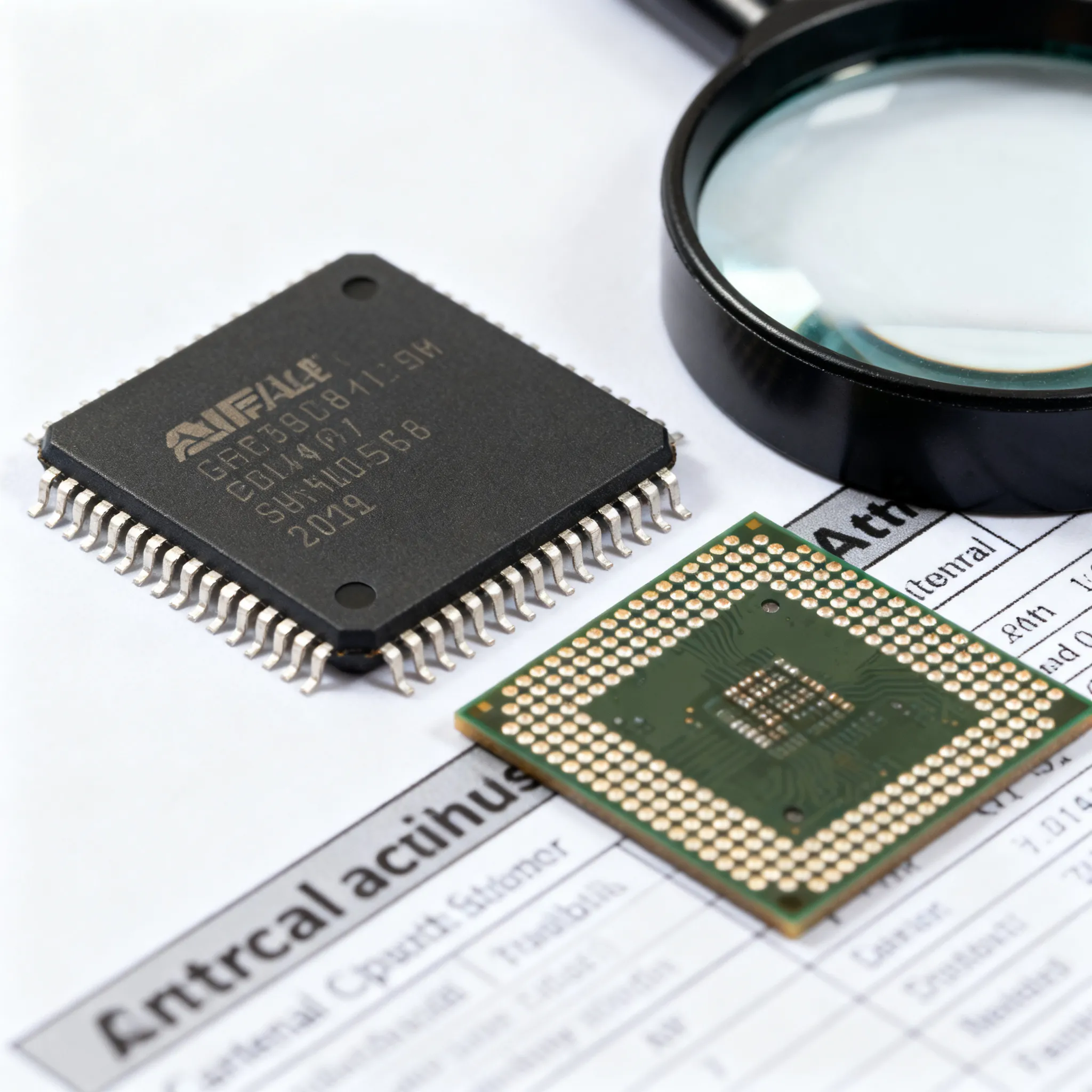
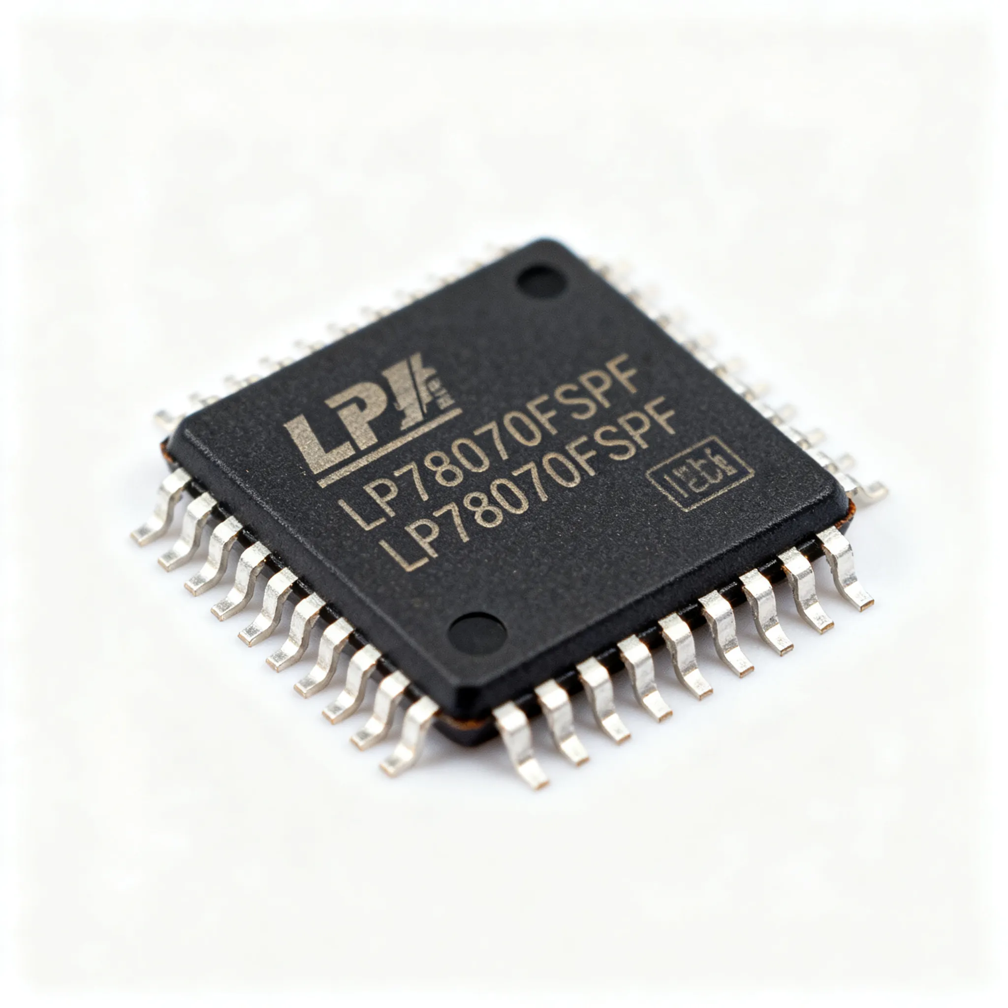
You will meet two main quad package families in consumer electronics design. The quad flat package, or QFP, is a surface-mounted integrated circuit package with gull-wing leads on all four sides. These leads are visible, so you can inspect solder joints quickly and catch defects during assembly. A QFP typically carries 32 to 200 pins, which supports microcontrollers, audio processors, and memory chips. Its flat, thin profile of about 1.5 to 3 mm fits slim devices such as televisions, laptops, and smartphones. Lead pitch options from 0.4 to 0.8 mm let you balance pin density against manufacturability. The ATmega328P in a 32-pin QFP, used on Arduino boards, shows how well a QFP suits prototyping and small production runs.
The quad flat no-leads package, or QFN, takes a different approach. A QFN is a leadless square package with an exposed thermal pad at its center. That pad solders directly to the board and pulls heat away from the die. Without long gull-wing leads, the QFN shrinks its footprint and shortens the electrical path. Nova Technology Company (HK) Limited, a HiSilicon-designated (authorized) solutions partner, supports customers who integrate such packages into chip-level solutions and full system integration. Variants extend the family further. A very-thin qfn reduces height for space-critical boards, and a flip-chip qfn connects the die directly to the substrate for even shorter interconnects.
LQFP and TQFP Variations
Two thinner QFP variations dominate thin consumer devices. The low-profile quad flat package, or LQFP, measures about 1.0 to 1.4 mm in body thickness. The thin quad flat package, or TQFP, measures about 1.0 to 1.2 mm. Both keep the gull-wing leads you already know from a standard QFP, so surface-mount technology lines handle them without special tooling.
Your choice between them depends on the production stage and the product. LQFP suits prototyping and early testing because its longer leads make soldering, inspection, and rework easier. LQFP also performs well in high pin count designs, where longer leads improve yield and solder reliability. TQFP fits mass production better, since automated assembly and compact layouts favor its lower profile. You will find TQFP in portable electronics, embedded microcontrollers, remote controls, compact sensors, and small modules. Both variations keep the quad package relevant across the full product lifecycle.
Miniaturization Benefits

Space-Saving Footprints
You save significant board space when you choose a qfn over a leaded package. The leadless design removes the gull-wing leads that extend outward from a qfp body. This change shrinks the footprint dramatically. Consider the numbers: a 2×2 mm qfn occupies just 4 mm², while an 8-lead SOIC needs 30 mm². That is 86% smaller. A 3×3 mm qfn stays under 10 mm², which is less than one third of the SOIC area. Weight drops too. The qfn weighs 0.0073 g, about 90% lighter than the SOIC at 0.077 g. You gain both space and mass savings for your compact size goals.
Wearable devices demand this level of miniaturization. A qfn starts at 2 mm × 2 mm, a size built for space-constrained products. The absence of leads makes the package more compact than any leaded alternative. Its thin profile supports slim designs. You also find micro leadframe qfn variants with heights from 0.35 mm to 1.45 mm. These options let you fit a qfn into tight enclosures without sacrificing performance. The qfp family offers its own space benefits. An LQFP has a low profile of 1.4 mm height. A TQFP is thinner than a standard qfp, which reduces vertical space in stacked designs. Both variations help you achieve a compact size in portable electronics.
High-Density PCB Layouts
Dense component placement becomes possible when you work with quad packages. A qfn uses perimeter I/O pads and a thermal pad, so you route signals around the edges without wasting interior space. A qfp exposes its pins along all four sides, which simplifies routing compared to BGAs. You can assemble these packages with a minimum fine pitch of 0.13 mm. That capability enables high-density interconnect designs in smartphones. For a 0.4 mm pitch qfn, manufacturers recommend 0.2 mm wide pads. This width avoids bridging between adjacent pads while maintaining acceptable solder contact. A 0.25 mm pad would reduce pin-to-pin spacing to 0.15 mm, a gap many designers consider too small.
The trend toward miniaturization continues across the industry. Over 58% of innovation in the electronic packaging market focuses on miniaturized formats, sustainable materials, and IoT devices. Electronics manufacturers represent about 64.9% of the market, leveraging advanced packaging for compact, high-performance products. Your printed circuit board design benefits from these advances. A qfn saves space and can reduce fabrication costs. A qfp remains easier to rework thanks to exposed leads. Both package types support higher component density and allow high-pin-count, low-pitch components. They also reduce signal path lengths, which improves signal quality. You should follow IPC-7351 standards and DFM requirements when you design for these packages. Via-in-pads help you route signals efficiently. With a quad package, you achieve the compact size and density that modern consumer devices require.
QFN Thermal and Electrical Performance

Heat Dissipation via Thermal Pad
A qfn solves a problem that troubles many small packages: heat has nowhere to go. The exposed thermal pad at the center of a quad flat no-leads package changes that. This pad solders directly to the PCB and creates a wide metal path from the die to the board. Heat flows out through the pad instead of building up inside the plastic body. You gain a cooler running integrated circuit and a longer product life.
You can strengthen this path with a thermal via array under the pad. A via-in-pad design might use 0.3 mm diameter vias at a 1.0 mm pitch. Studies suggest a well-designed thermal via array can reduce thermal resistance by up to 50%, which significantly lowers component temperatures. Copper-filled vias help further. They replace trapped air with solid copper and can cut thermal resistance by 20-30% compared to unfilled vias. A copper plane of 1 oz/ft² (35 μm) or more acts as an effective heat spreader.
Follow these design rules when you lay out a qfn:
- Choose via diameters between 0.2 mm and 0.4 mm (8–16 mil).
- Maintain 1–1.2 mm (40 to 48 mil) via-to-via distance to prevent solder wicking.
- Keep the via aspect ratio below 10:1 for uniform copper plating.
- Connect vias to large copper planes to spread heat and reduce hotspots.
For QFN and DFN packages, follow the datasheet guidelines for thermal via placement due to exposed thermal pads.
Short Signal Paths for Efficiency
A qfn removes the long gull-wing leads you see on a qfp. That single change shortens every electrical path between the die and the board. Shorter paths mean less resistance, less inductance, and less signal loss. Your high performance circuits keep more of their margin. A qfp still performs well, yet its leads add length that a qfn avoids.
These short paths protect signal integrity in several ways. They reduce parasitic capacitance and inductance, so fast edges stay clean. They lower crosstalk between adjacent pins. They also cut electromagnetic interference, which matters in dense boards. A designer who fights signal integrity problems often finds relief in a qfn layout.
The leadless body helps in another way. A quad flat no-leads package places its pads right at the package edge, so you route traces with minimal stub length. A qfp gives you inspectable leads and easier rework, a real advantage during prototyping. A qfn wins when speed and density matter most. Both packages support high performance designs, and both appear in consumer products every day. Your choice depends on the trade-off between assembly convenience and electrical efficiency. For a compact, high performance device, the qfn usually leads.
Manufacturability and Cost
SMT Assembly Ease
You will find both package families ready for standard surface-mount technology lines. A qfp uses gull-wing leads that sit on visible pads, so automated assembly equipment places and solders them with mature, well-understood processes. Solder joint inspection happens visually or with automated optical tools, which keeps quality control straightforward. A quad flat no-leads package takes a different path. Its leadless pads sit underneath the body, so you rely on X-ray inspection instead of visual checks. A wettable flank qfn improves this situation. The wettable flank qfn adds plated edges that allow some optical solder joint inspection after reflow.
Cost tells a clear story in high-volume production. A qfn carries a lower unit price because its simpler structure uses less material. A qfp costs slightly more per unit thanks to its mature process and additional lead frame material. The table below shows typical ranges.
| Package Type | Cost per Unit (USD) |
|---|---|
| QFN | $0.10 – $0.50 |
| QFP | $0.50 – $2.00 |
You gain cost-effective manufacturing when you match the package to the product. A qfn wins on material savings. A qfp wins on process maturity and easy rework.
PCB Design for QFN Packages
Good pcb design for qfn packages starts with the thermal pad. Divide the exposed pad into smaller rectangles, such as a 3x5 or 5x5 grid. This pattern creates gas bleed-out paths during reflow while maintaining thermal continuity. Verify tolerances using IPC-7351 producibility levels. For high-reliability builds, choose Level 2 or 3.
Solder paste volume control matters just as much. Target 50–80% paste coverage of the pad area. Use window-pane stencil patterns with openings occupying 60–75% of the pad. A stencil thickness of 0.1–0.125 mm suits fine-pitch qfn packages, with Type 4 or finer paste particles. Plug thermal vias with copper plating, epoxy filling, or solder mask tenting to prevent solder wicking. Limit via diameter to 0.3 mm or smaller. These steps protect signal integrity and reduce voiding. For components dissipating more than 10W, thermal vias alone may not suffice. You then need heat sinks or forced air. Always follow IPC-7095 via-in-pad guidance for bottom-terminated components. A printed circuit board designed this way supports reliable automated assembly and strong signal integrity across the product life.
Consumer Electronics Applications
Smartphones and Tablets
Your smartphone packs dozens of chips into a slim frame. Quad packages make that possible. A qfp handles the main processor in many tablets, where its gull-wing leads simplify board rework during production. A qfn takes over where space matters most. Power management integrated circuit chips commonly use a 32-pin qfn measuring 4x4 mm, and that package dissipates 2 W of heat. RF transceivers and 5G modules also rely on qfn packaging because its low parasitics support high performance at speed.
The table below shows where you find these packages in a typical phone.
| Smartphone IC type | Package | Details |
|---|---|---|
| Power management ICs | 32-pin qfn | 4x4 mm size; 2 W heat dissipation |
| RF transceivers | qfn | Low parasitics for high-speed applications |
| 5G modules | qfn | Low parasitics for high-speed applications |
A qfp also serves memory and audio controllers in tablets. The package family has deep roots in consumer devices.
The first QFPs were introduced in Japan in 1977 to allow more pins for electronic calculators, and the package soon spread to other consumer electronics in that country.
That history explains why a qfp remains a familiar sight on circuit boards today.
Wearables and IoT
Wearables demand a compact size and low power above all else. A qfn delivers both. The BG29 Bluetooth LE integrated circuit comes in qfn packages, which suit devices like pulse oximeters and heart rate monitors. The BG22 TQFN package measures only 0.3 mm thick, and that thin profile enables slimmer PCB architectures for wearable devices. You gain a compact size without sacrificing high performance.
IoT sensors follow the same logic. A qfn fits into tight enclosures, and its short signal paths keep power draw low. A qfp still appears in gateway modules and smart home hubs, where board space is less constrained. For high-performance electronics, the qfn often wins the wearable socket. Nova Technology Company (HK) Limited, a HiSilicon-designated (authorized) solutions partner, supports customers who integrate these packages into chip-level solutions and full system integration. Whether you design a fitness band or a smart thermostat, the quad package gives you a compact size and the high performance your product needs.
Quad Flat Package vs. Other Types
BGAs and SOPs Comparison
When you compare quad packages to other surface-mount options, two types come up often: BGAs and SOPs.
Ball grid arrays (BGAs) offer higher pin densities than a qfp. A BGA places solder balls under the package body, which gives you more I/O connections in the same footprint. However, BGAs require X-ray inspection for solder joint verification. Rework on a BGA is more difficult and expensive. A qfp gives you visible gull-wing leads on all four sides, so automated assembly lines inspect them with standard optical tools. Rework stays straightforward. For cost-sensitive consumer products, a qfp often wins over a BGA. Your signal integrity remains easier to manage with a qfp because the leads stay accessible for testing.
Small outline packages (SOPs) use a simpler design. An SOP has leads on two sides only, which limits its pin count. A quad flat package handles up to 304 leads, while an SOP typically maxes out at 48 pins. You choose a qfp when your component needs more connections. A qfp also dissipates more heat than an SOP, which makes it better for systems that generate moderate heat. High performance chips like processors and graphics cards use qfp packaging. The qfp supports your high performance goals without the thermal limits of an SOP.
Best Choice Scenarios
You select a quad flat package in several common scenarios. When your design requires between 32 and 200 pins, a qfp provides inspectable joints, mature automated assembly processes, and low cost. When you need a leadless package for space-critical boards, a qfn shrinks the footprint and improves signal integrity with short electrical paths.
The quad package suits consumer electronics where balanced performance matters. You get enough pins for complex chips without the cost of a BGA. You gain better heat dissipation than an SOP. Your signal integrity improves because the short lead paths in a qfn reduce parasitic effects. The qfp also delivers strong signal integrity for medium-speed designs. For high performance designs in smartphones, wearables, and IoT devices, this package family delivers the right mix of density, thermal capability, and automated assembly compatibility.
You now see why the quad package wins in consumer electronics. A qfp gives you inspectable leads, low cost, and mature assembly. A qfn shrinks the footprint and moves heat through its thermal pad. Both deliver a compact size, strong thermal performance, and easy surface-mount assembly. A qfp keeps rework simple. A qfn saves board space. A qfp suits medium pin counts. A qfn serves dense, fast designs. A qfp and a qfn each cut unit cost in high volume. The quad flat package enables the slim, powerful, affordable devices you use daily. The quad flat package will keep shaping future designs. Expect a qfp and a qfn in tomorrow's compact size, high performance products.
FAQ
How do you choose between a QFP and a QFN?
Match the package to your priorities. A qfp gives you visible gull-wing leads, easy rework, and pin counts from 32 to 200. A qfn saves board space and shortens signal paths. Pick a qfp for prototyping and medium pin counts. Pick a qfn for dense, fast designs.
What does the thermal pad do in a QFN?
The exposed pad at the center solders straight to the board. Heat leaves the die through this wide metal path instead of building up inside the plastic body. A thermal via array under the pad strengthens that path further. Your chip runs cooler and lasts longer.
Why do wearables often use QFN packages?
Wearables need small size and low power. A qfn starts at 2 mm × 2 mm, and thin variants measure only 0.3 mm in height. Short signal paths cut parasitic losses, which keeps power draw low. A qfp still works in gateway modules where board space is less tight.
Can you rework a QFP more easily than a QFN?
Yes. A qfp exposes its gull-wing leads on all four sides, so you inspect and rework solder joints with standard tools. A qfn hides its pads under the body, so you need X-ray inspection. A wettable flank qfn adds plated edges that allow some optical checks after reflow.
Do quad packages cost more than other options?
No. A qfn carries a lower unit price because its simpler structure uses less material. A qfp costs slightly more per unit, yet it still beats a BGA for cost-sensitive products. Both packages keep automated assembly costs low in high-volume production.