High-Resolution Photos of Integrated Circuits and Their Insights into Semiconductor Design
High-resolution photos give us a clear look at semiconductors. These pictures show tiny details inside each integrated circuit. Engineers and researchers use these photos to study chips.
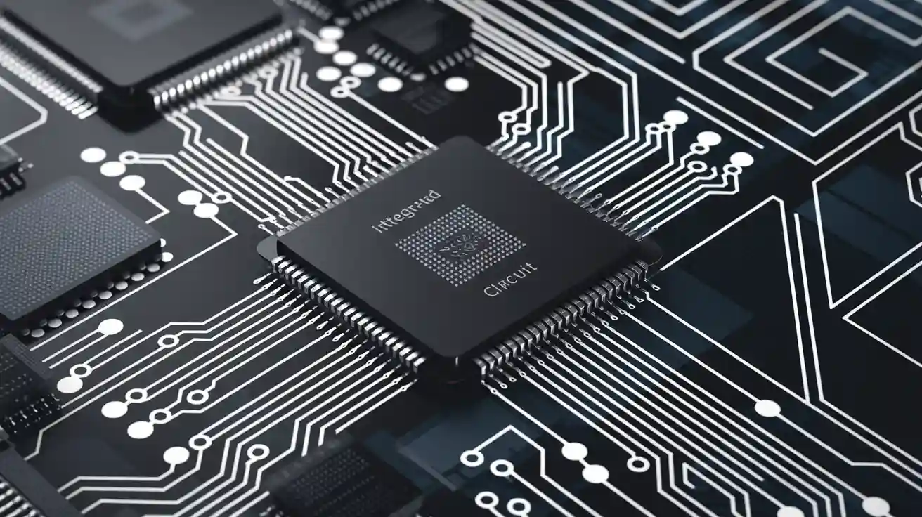
High-resolution photos give us a clear look at semiconductors. These pictures show tiny details inside each integrated circuit. Engineers and researchers use these photos to study chips. They help people learn how semiconductor technology works. The semiconductor industry needs these photos to see layers and patterns. These layers and patterns make each integrated circuit special. Students can learn about design choices by looking at these images. They also learn about the industry. High-resolution photos help people see how complex semiconductors are. They show why design is important in modern chips.
Key Takeaways
-
High-resolution photos show small parts inside integrated circuits. These photos help engineers and students learn about chip design and structure. Advanced imaging tools and deep learning make photos clearer and faster to take. This lets people see complex semiconductor layers more easily. These images help find problems early and make chips better. They also help create new ideas in design and manufacturing. High-resolution photos help schools and companies work together. This teamwork brings new ideas and better technology to the semiconductor industry. Security experts use these photos to spot fake or changed chips. This helps keep internet-connected devices safe and working well.
High-Resolution Photos Explained
Definition and Access
High-resolution photos help people in the semiconductor industry look inside chips. These pictures are made using special imaging tools like 3D X-ray microscopes and scanning electron microscopes. Engineers use these machines in labs to see every tiny part inside semiconductors. Some companies let people get these images from stock photo websites or industry databases.
The semiconductor industry uses these photos to learn about chip design, how chips are made, and new ideas. Imaging technology now uses deep learning to make photos faster and clearer. For example, 3D X-ray microscopes with deep learning can scan a big chip area at low resolution. Then, they make the image much sharper. This helps engineers see more of the chip in less time. The table below shows how these tools make integrated circuit photos better and more detailed:
|
Aspect |
Description |
Quantitative Impact |
|---|---|---|
|
Imaging Technology |
3D X-ray microscopy with deep learning reconstruction |
Multi-scale imaging and resolution enhancement |
|
Voxel Resolutions |
Low-res: 0.53 µm/voxel; High-res: 0.26 µm/voxel |
Upscales low-res data to high-res level |
|
Volume Coverage |
Upscales low-res volume to high-res equivalent |
~8 times larger analyzable volume |
|
Acquisition Time |
Single high-res scan: 1.5 hours; DeepScout scan: a few hours |
Faster scans with more detail |
|
Image Quality |
Deep learning for noise removal and denoising |
Sub-micrometer resolution and clearer images |
|
Application Benefits |
Non-destructive 3D imaging of complex integrated circuits |
Better failure analysis and quality assurance |
People measure image quality using things like Peak Signal-to-Noise Ratio (PSNR), Structural Similarity Index (SSIM), and Visual Information Fidelity (VIF). These help the industry check if the photos are good enough for research and making chips.
Revealing IC Structures
High-resolution photos show the many layers inside semiconductors. Imaging tools like ptychographic X-ray laminography can show parts called interconnects that are only 30 nanometers apart. Some scans can even show details as small as 19 nanometers over a 40-micrometer chip area. These images let engineers see each layer of an integrated circuit without breaking the chip. They can find problems, study how the chip is built, and see how making chips changes their design.
Imaging software can highlight different layers or features, like how HDR video shows bright and dark spots. This helps the semiconductor industry learn more about chip design and how chips are made. High-resolution photos help engineers and researchers find problems, make chips better, and come up with new ideas. These images also help students learn by showing them what semiconductors really look like and how technology changes modern chips.
Insights from Integrated Circuit Design
Layout and Architecture
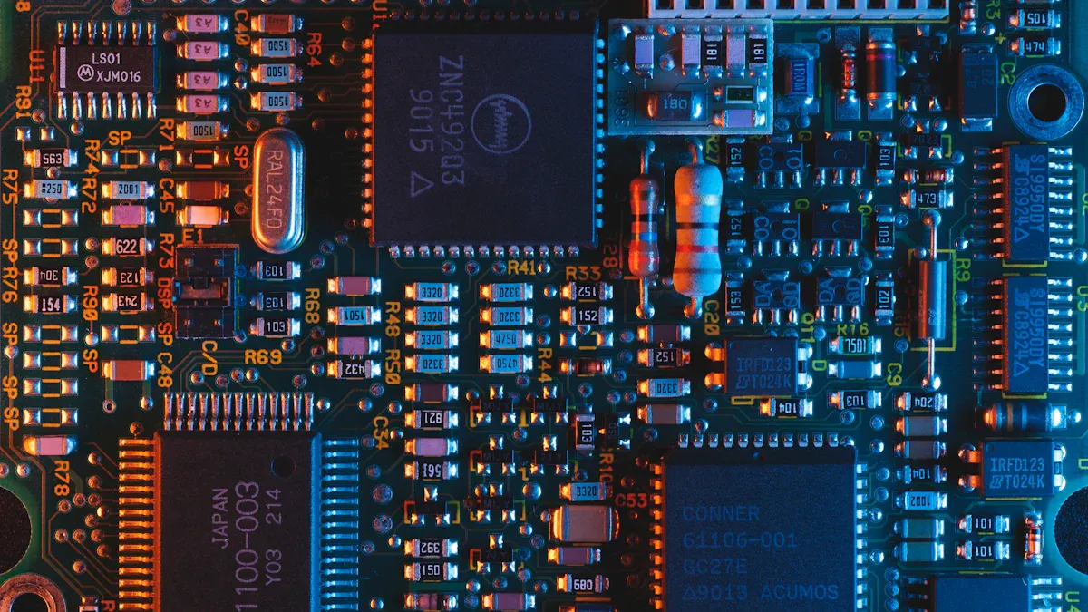
High-resolution photos let engineers see the layout of semiconductors up close. These images show how designers put circuits and parts inside chips. Each layer in a semiconductor does something special. Some layers move signals. Other layers give power or link different parts. Engineers look at these photos to learn about chip architecture. They see how all the parts fit together.
The semiconductor industry uses these images to check if layouts match the plans. Engineers can find mistakes or changes from making the chips. Photos also show how designers use space inside chips. Good layouts help chips run faster and use less energy. The industry uses what they learn to make better chip designs and products.
Note: High-resolution images help students and new engineers see how complex chip architecture works. They can look at real examples of what semiconductors look like inside.
Design Trends and Innovations
The global semiconductor market changes fast. High-resolution photos help experts watch new trends. Lately, engineers use 3D stacking in chip design. This puts layers of circuits on top of each other. It saves space and makes chips work faster. High-resolution images show how these layers connect.
Another trend is using artificial intelligence in electronic design automation. AI tools help engineers make better designs by finding patterns in high-resolution images. These tools can find problems or suggest new ways to arrange circuits. The industry uses these ideas to keep up with new technology.
In 2024, Audio & Video Processing made up over 63.7% of the Multimedia IC market. This happened because people want chips for 4K and 8K content. The Consumer Electronics segment, like smartphones with good cameras and screens, had more than 72.6% of the market. These numbers show that high-resolution imaging and new chip design are closely linked. Companies make chips that handle better images and videos. This trend helps the whole industry grow.
Manufacturing and Defects
Making semiconductors is hard. High-resolution photos help find defects and changes in chips. These images can show tiny cracks, missing links, or small particles. Engineers use this to fix problems before chips go to customers.
The industry uses these photos to check quality. They compare finished chips to the plans. If they see differences, they can find out where things went wrong. This helps companies make better chips and waste less.
Tip: High-resolution photos help spot defects too small for regular tools. This helps the industry keep quality high and costs low.
Engineers also use these images to see how new materials and ways of making chips change how they work. They can see if changes make chips better or worse. These ideas help the industry follow new trends and stay ahead.
Real-World Applications
Research and Education
High-resolution photos are important in labs and schools. Scientists use these images to learn how semiconductors work. They often use machines like the OT-2 robotic liquid handler to get samples ready. This saves time and helps them get better results. Labs use automated staining and high-content imaging to look at DNA damage in cells. Deep learning tools help them study these images faster. Students look at real chip photos to learn about semiconductors. Teachers use these images to show how the industry makes new technology. Data management systems keep the images sorted and easy to find. This helps research go faster and be more trustworthy.
-
Automated imaging platforms help labs go from sample prep to taking pictures quickly.
-
Deep learning makes image study faster and helps find patterns.
-
Automation means less manual work and more experiments can be done.
Industry Analysis
The semiconductor industry uses high-resolution imaging to study materials and make products better. Companies use advanced STEM techniques to see atoms inside semiconductors. They map where atoms are in materials like GaAs1−xBix. These images help the industry see how elements mix in chips. Electric field mapping shows how charge moves in devices. The industry uses 3D chemical maps to find defects and make manufacturing better. At the china international semiconductor expo, experts share new imaging ideas and results. They show how these tools help make better chips for iot and other uses. The industry also looks at nanowires and thin films to find new ways to build semiconductors.
-
Combined imaging modes give clear views of complex alloys.
-
In situ analysis lets the industry watch changes as chips are made.
-
The china international semiconductor expo shows the newest imaging technology for the industry.
Security and Reverse Engineering
Security experts use high-resolution photos to check if chips are safe. They look for hidden changes or fake parts in semiconductors. The industry needs these checks to keep iot devices safe. Reverse engineers use these images to learn how a chip works. They can see if someone copied a design or changed it. At the china international semiconductor expo, security teams show how imaging keeps the industry safe. The industry uses these tools to stop fake chips and protect new technology. High-resolution imaging helps the industry make sure semiconductors are safe.
Note: High-resolution imaging helps the industry keep up with new threats and protect iot devices.
Impact on Semiconductor Development
Design Improvement
High-resolution photos help make chip design better. Engineers use these images to see tiny details inside semiconductors. They can find small problems that might slow down a chip or make it fail. If engineers spot these issues early, they can fix them before selling the chip. This saves both time and money for companies.
New technology like deep learning makes these images even clearer. For example, in medical imaging, the NexGen 7T MRI scanner made 3D images ten times sharper than older ones. This happened because engineers used better designs and new receiver arrays. The same idea works for semiconductors. High-resolution images let engineers see layers and circuits that were hidden before. This helps them make better and stronger chips for iot devices.
Deep learning also makes PET scans look sharper. The semiconductor industry uses similar tricks to make chip images better. These changes help engineers build chips that work well in the internet of things and other areas.
Tip: High-resolution imaging lets engineers see the smallest parts of semiconductors. This makes it easier to improve design and architecture for iot and more.
Innovation and Collaboration
The semiconductor industry grows faster when people work together. Schools and companies often team up to solve big chip problems. High-resolution images help everyone share ideas and learn new things. These images make it easier to study new materials, test new designs, and find better ways to build chips for the internet of things.
|
Collaboration Program/Consortium |
Lead Academic Institution(s) |
Industry Partners |
Funding Amount |
Key Goals/Impact on Integrated Circuits |
|---|---|---|---|---|
|
North Texas Semiconductor Institute (NTxSI) |
University of Texas at Dallas (UT Dallas) |
Texas Instruments, Global Wafers, Coherent, Qorvo, Wolfspeed, NXP, Infineon, others |
N/A |
Workforce development, semiconductor research, device support, startup support |
|
North Texas Semiconductor Workforce Development Consortium (NTS-WDC) |
Multiple academic institutions including UT Dallas, Collin College, Dallas College, Grayson College, North Central Texas College, Texas State Technical College, University of Texas at Arlington |
Texas Instruments, Global Wafers, other key industry members |
$3 million (Department of Education) |
Increase engineering technology certificate and degree output 3x over 3 years; align workforce skills with industry needs |
|
Texas Analog Center of Excellence (TxACE) |
UT Dallas, University of Texas System |
Texas Instruments, Semiconductor Research Corporation, State of Texas |
N/A |
Research and development of analog integrated circuits critical to $550+ billion integrated circuits industry; supports imaging, sensing, communication, power management |
These partnerships help train new workers, support startups, and push new ideas in semiconductors. High-resolution imaging gives both schools and companies the tools to study chips for iot and other uses. Working together leads to better technology and stronger products for everyone.
High-resolution photos let us see inside integrated circuits. These pictures show what is hidden in chips. Engineers, students, and researchers use them to learn about semiconductors. The images show small details, new designs, and possible problems. People look at these photos to learn and fix issues. They also help make better technology.
Looking at these images can give people new ideas. They can make you curious about how electronics change our world.
-
Engineers make chip designs better.
-
Students look at real chip examples.
-
The industry finds new ways to improve.
FAQ
What makes high-resolution photos important for semiconductors?
High-resolution photos let engineers and students see small details. These images show layers, patterns, and problems inside semiconductors. They help people understand chip design and how chips are made. The photos also show new ideas in the semiconductor industry.
How do high-resolution photos support chip design and architecture?
Engineers look at high-resolution photos to study chip layout. The images show how circuits and layers are put together. By looking at these photos, people find ways to make chips better and faster.
What role do high-resolution photos play in the global semiconductor market?
The global semiconductor market uses high-resolution photos to watch new trends. Companies use these images to check new technology and see if chips are made well. They also share these photos at big events like the china international semiconductor expo.
How do high-resolution photos help with security and the internet of things?
Security experts use high-resolution photos to check chips for hidden changes. These images help keep iot devices safe by finding fake parts or mistakes in integrated circuits.
Can high-resolution photos drive innovation in the semiconductor industry?
High-resolution photos give the industry new ideas. They help researchers and engineers find problems and test new designs. These images help people make better technology and stronger chips for the future.