Understanding the 16V 1mf SMD 4x5.4mm Electrolytic Capacitor in KiCad
A 16v 1mf smd 4 x 5.4mm electrolytic capacitor kicad serves as a compact energy storage device in modern PCB designs. Engine
A 16v 1mf smd 4 x 5.4mm electrolytic capacitor kicad serves as a compact energy storage device in modern PCB designs. Engineers select voltage ratings at least 50% higher than the circuit’s maximum to prevent breakdown. They choose capacitance with a margin above the minimum to account for tolerance and aging. Physical size helps manage heat and ripple current. KiCad supports precise integration by matching schematic symbols and footprints. Polarity and footprint alignment ensure stable and safe circuit operation.
Key Takeaways
- Choose a capacitor with voltage at least 50% higher than your circuit’s max to avoid damage.
- Match the 4x5.4mm package size carefully in KiCad to ensure the capacitor fits and works well.
- Always check and mark capacitor polarity to prevent failures and extend circuit life.
- Use KiCad’s symbol and footprint libraries or create custom footprints when needed for accuracy.
- Run design rule checks and verify placement to catch errors before manufacturing.
Specifications

Voltage and Capacitance
Engineers select voltage and capacitance based on the needs of the circuit. The 16V rating allows the capacitor to handle moderate voltage levels, making it suitable for power supplies and audio equipment. Capacitance of 1 µF helps filter noise and stabilize voltage. The following table shows standard ratings for SMD electrolytic capacitors in consumer electronics:
| Parameter | Range | Typical Application / Notes |
|---|---|---|
| Voltage Rating | 6.3V to 10V | Smartphones, tablets; low voltage, compact size. |
| 16V to 25V | Power supplies, audio gear; moderate voltage tolerance. | |
| 35V to 50V | Power management, industrial electronics; high voltage tolerance. | |
| Capacitance Value | 1 µF to 10 µF | Decoupling, filtering high-frequency noise; compact, low ESR. |
| 22 µF to 100 µF | Filtering, energy storage in power supply circuits. | |
| 100 µF to 470 µF | Bulk energy storage, smoothing in power supplies and audio equipment. |
Larger SMD electrolytic capacitors maintain capacitance better under DC bias and handle ripple current more effectively. Smaller packages offer improved high-frequency performance due to lower parasitic inductance.
SMD Package and Size
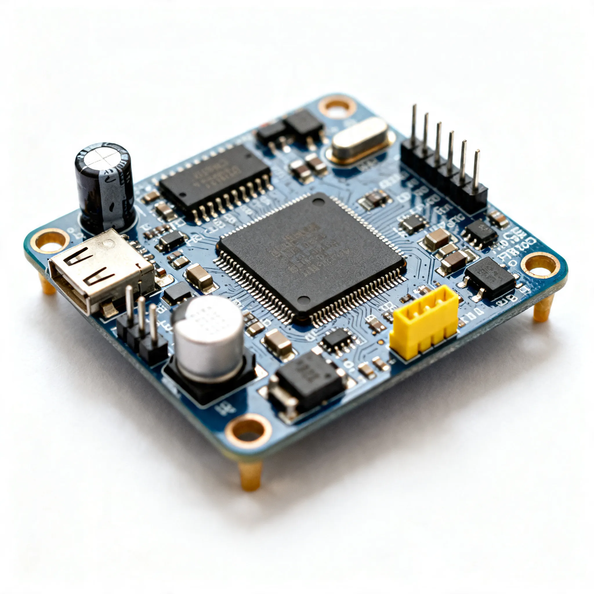
The 4x5.4mm SMD package balances size and performance. This footprint fits many general-purpose and industrial applications. Devices such as medical equipment, automotive electronics, and control systems use this size for reliable filtering and coupling. The 4x5.4mm package provides mechanical stability and good thermal performance. Engineers compare it to similar sizes, such as 4.0mm x 5.8mm, to ensure compatibility and optimal performance. Proper footprint matching in KiCad ensures the 16v 1mf smd 4 x 5.4mm electrolytic capacitor kicad fits securely and functions as intended.
Tip: Always check the datasheet for exact dimensions and recommended PCB footprint to avoid assembly errors.
Polarity
SMD electrolytic capacitors are polarized. Manufacturers mark the negative terminal with a stripe and sometimes a minus sign. Industry standards, such as IPC-7351B, require clear polarity indication on both the capacitor and the PCB silkscreen. Silkscreen symbols, like stripes or plus signs, help prevent placement mistakes. Engineers verify polarity by reviewing silkscreen, schematic, and placement drawings. Incorrect polarity causes dielectric breakdown, short circuits, and heat generation. These failures can damage the capacitor and surrounding components, reducing circuit reliability. Proper polarity identification and adherence ensure long operational life and safe performance.
- Polarity reversal leads to catastrophic failures, including explosion or leakage.
- Incorrect polarity accelerates aging, causing loss of capacitance and increased leakage current.
- Voltage derating and thermal management improve lifespan and reliability.
16v 1mf smd 4 x 5.4mm Electrolytic Capacitor KiCad Integration
Symbol Selection
Selecting the correct symbol for a 16v 1mf smd 4 x 5.4mm electrolytic capacitor kicad in KiCad helps engineers avoid confusion and errors during design. They follow these steps:
- They check the physical dimensions of the capacitor, making sure it matches the 4x5.4mm size.
- They search KiCad’s symbol library for an electrolytic capacitor symbol. The symbol should show polarity, with a clear marking for the negative terminal.
- They separate the capacitance and voltage values. For example, they enter "1µF" in the value field and "16V" in an extra field. This method keeps the schematic clear and helps with simulation.
- They link the symbol to the datasheet using the Datasheet field. This link lets them quickly check manufacturer specifications.
- They sync the symbol with database libraries to keep component values and placement consistent.
Tip: Engineers often use manufacturer websites or trusted distributors like Digi-Key to find accurate KiCad models and 3D files for their capacitors.
Footprint Matching
Footprint matching ensures that the 16v 1mf smd 4 x 5.4mm electrolytic capacitor kicad fits perfectly on the PCB. Engineers use these steps:
- They read the capacitor’s datasheet to confirm the exact size and voltage rating.
- They assign the correct footprint in KiCad, matching the 4x5.4mm SMD package.
- If the footprint is missing, they download a custom footprint from trusted sources or create one based on datasheet dimensions.
- They place the footprint near power lines or areas needing voltage smoothing.
- They run KiCad’s design rule check to catch mismatches or errors early.
- They check polarity markings on both the footprint and the PCB silkscreen. The negative terminal must match the stripe on the capacitor.
| Parameter Type | Description |
|---|---|
| Manufacturer | Identifies the capacitor’s brand |
| Case Size (X x Y) | Shows the physical size, such as 4 x 5.4mm |
| Height (H) | Indicates the height of the capacitor |
| Pitch (P) | Displays the lead spacing |
| Modifiers | Lists any special features |
| Options | Provides extra footprint choices |
This table helps engineers match datasheet details with KiCad footprint entries. They use these fields to make sure the footprint fits the real component.
Note: Engineers avoid mistakes by checking the datasheet for pin assignments and comparing them with the symbol’s pin numbers in KiCad.
Library Search
Engineers search for verified symbols and footprints in KiCad libraries using several resources:
- IPC standards, such as IPC7351B, guide footprint naming and design for manufacturability.
- Mentor Graphics LP-Viewer offers footprints that follow IPC recommendations, using the "CAPAE" naming for SMD electrolytic capacitors.
- Datasheets provide exact dimensions and help create custom footprints when needed.
- JEDEC standards and Altium’s libraries also support footprint searches.
- Custom footprint creation is common when verified KiCad footprints are not available.
Engineers often join KiCad forums, watch tutorials, and read datasheets to improve their skills and accuracy. They learn to cross-reference datasheet information with KiCad library entries by checking case size codes and matching them with the footprint’s dimensions.
By following these steps, engineers ensure that the 16v 1mf smd 4 x 5.4mm electrolytic capacitor kicad is correctly represented in both the schematic and PCB layout. They use datasheets and marking codes to verify every detail, reducing the risk of assembly errors and improving circuit reliability.
Custom Footprint Creation
When to Create Custom Footprints
Engineers sometimes cannot find the exact footprint for a capacitor in KiCad’s standard libraries. They need to create a custom footprint when the capacitor’s size, shape, or pin spacing does not match any available options. For SMD electrolytic capacitors, important features like diameter, height, and pitch must match the datasheet. Polarized capacitors also require clear polarity markings on the footprint. Custom footprints help ensure the component fits the board and works as expected.
Tip: Always check the datasheet for the capacitor’s exact measurements before starting a custom footprint.
Common reasons for custom footprint creation include:
- The standard library does not have the correct size or shape.
- The datasheet shows unique dimensions or lead spacing.
- The capacitor is polarized and needs special orientation markings.
- The design requires exact pad positions for reliable soldering.
- Engineers want to match the schematic symbol to the new footprint for accuracy.
Steps in KiCad
KiCad makes it possible to create or edit footprints with precise control. Engineers follow these steps:
- Set the units in KiCad to millimeters to match the datasheet.
- Use the "Add Pad" tool to place pads for the capacitor’s terminals.
- Open the pad properties dialog by right-clicking or pressing ‘E’ on a pad.
- Enter the pad type (SMD), number, shape, and exact size.
- Position pads using grid snapping or by entering X and Y coordinates.
- Draw the component outline and polarity markings on the silkscreen and courtyard layers.
- Save the new footprint and assign it to the schematic symbol.
The table below lists important parameters to consider when designing a custom footprint for a 4x5.4mm SMD electrolytic capacitor:
| Parameter | Description & Importance |
|---|---|
| Physical Dimensions | 4x5.4mm size must match the PCB for proper placement. |
| Surface Mount Land Size | Pad size and spacing ensure good soldering and stability. |
| Polarity | Markings show correct orientation to avoid damage. |
| Number of Terminations | Two pads for standard electrolytic capacitors. |
| Tolerance | ±20% is common; affects performance. |
| Moisture Sensitivity Level (MSL) | Level 1 means low risk during storage and soldering. |
Editing Existing Footprints
Sometimes, engineers only need to adjust an existing footprint. They can change pad sizes and polarity markings in KiCad by selecting a pad and opening the properties dialog. This dialog lets them set the pad’s size, shape, and number. Engineers use the silkscreen layer for visible polarity marks and the fabrication layer for detailed outlines. They make sure the pad numbers match the schematic symbol. Courtyard lines define the space needed for assembly.
Note: Consistent units and careful layer management help avoid mistakes when editing footprints.
A well-edited footprint for a 16v 1mf smd 4 x 5.4mm electrolytic capacitor kicad ensures the component fits, works safely, and is easy to assemble.
Placement and Verification
PCB Placement
Engineers place SMD electrolytic capacitors close to the circuits that need stable voltage or noise filtering. They avoid placing the capacitor near heat sources or in tight spaces where airflow is limited. Good placement helps the capacitor work longer and keeps the circuit safe. They check the datasheet for the recommended footprint and spacing. This step prevents problems during assembly. Engineers also make sure the 16v 1mf smd 4 x 5.4mm electrolytic capacitor kicad does not block other components or test points.
Tip: Place the capacitor so that the silkscreen markings are visible after assembly. This makes inspection and troubleshooting easier.
Orientation and Polarity Check
SMD electrolytic capacitors have clear polarity markings. The positive terminal often has a '+' sign or a colored stripe. The negative terminal usually matches a filled area on the PCB silkscreen. Engineers follow these steps to check orientation and polarity:
- Look for the '+' sign or colored stripe on the capacitor body.
- Match the negative lead with the filled area on the PCB silkscreen.
- Double-check the datasheet for polarity details.
- Use a multimeter if unsure about the markings.
- Confirm that the silkscreen labels on the PCB match the capacitor’s markings.
- Buy capacitors from trusted suppliers to avoid marking errors.
Incorrect polarity can cause the capacitor to fail or even explode. Engineers always verify orientation before soldering.
Design Rule Check
Design rule checks (DRC) help engineers find mistakes before manufacturing. They use these checks to make sure the capacitor fits and works safely. Important steps include:
- Check that all polarized capacitors have clear orientation markers.
- Make sure silkscreen layers show polarity for easy inspection.
- Run DRC to confirm minimum spacing between pads and traces, usually at least 6 mils.
- Verify that pad sizes and annular rings meet the manufacturer’s minimum requirements.
- Compare the design with the manufacturer’s capability matrix.
- Generate 3D models to check mechanical fit and clearance.
- Use DFM tools to catch errors that could cause problems during assembly.
Engineers run these checks often during the design process. This practice helps avoid costly mistakes and ensures the board is ready for manufacturing.
Engineers follow several key steps to integrate SMD electrolytic capacitors in KiCad. They match the correct footprint, check polarity, and use design rule checks to catch errors.
- Common mistakes include using the wrong footprint size, missing polarity marks, or not keeping enough space between components.
- Experts recommend reviewing datasheets, verifying pin numbers, and using automated inspection tools for accuracy.
Always consult datasheets and double-check footprints before sending a PCB design to production. Careful review helps prevent costly assembly errors.
FAQ
What does "4x5.4mm" mean for an SMD electrolytic capacitor?
"4x5.4mm" shows the physical size of the capacitor. The first number is the diameter (4mm). The second number is the height (5.4mm). This size helps engineers pick the right footprint in KiCad.
How can someone check capacitor polarity in KiCad?
Engineers look for a stripe or minus sign on the symbol and footprint. The negative terminal matches the stripe on the real capacitor. KiCad’s silkscreen layer also shows polarity marks for easy checking.
Why is matching the footprint size important?
A correct footprint ensures the capacitor fits on the PCB. If the size does not match, the part may not solder well or could cause short circuits. Engineers always check the datasheet before choosing a footprint.
Can KiCad create custom footprints for unique capacitor sizes?
Yes, KiCad lets users design custom footprints. Engineers enter the exact pad size and spacing from the datasheet. They add polarity marks and save the new footprint for future use.
What happens if someone installs the capacitor backwards?
Installing the capacitor with reversed polarity can cause it to fail. The part may leak, overheat, or even explode. Engineers always double-check polarity before soldering.