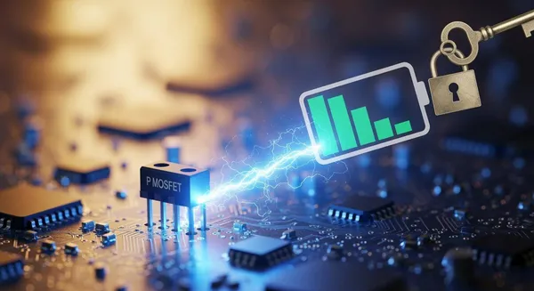
Unlock Better Battery Life with a P Channel MOSFET
P-channel MOSFETs are a key to achieving longer battery life. These special p-channel mosfets enable simpler and m
P-channel MOSFETs are a key to achieving longer battery life. These special p-channel mosfets enable simpler and more efficient high-side power switching. This p-channel method is ideal for power-gating in battery-powered devices. It drastically reduces standby power draw and simplifies the overall circuit design compared to other types of mosfets.
The p channel mosfet is more than just a component. It is a strategic design choice for maximizing energy efficiency. This p-channel technology and its simple control make the p-channel mosfet a cornerstone of efficient power management in a growing market. This p-channel mosfet is a powerful mosfet.
Key Takeaways
- P-channel MOSFETs improve battery life. They simplify power control in devices. This reduces standby power use.
- P-channel MOSFETs are best for high-side switching. They turn on easily with a microcontroller. This avoids complex circuits.
- P-channel MOSFETs are useful in many devices. They help in IoT, wearables, and electric vehicles. They manage power efficiently.
- Choose a P-channel MOSFET with low Rds(on). This reduces wasted power. It also helps with logic-level Vgs(th) for direct control.
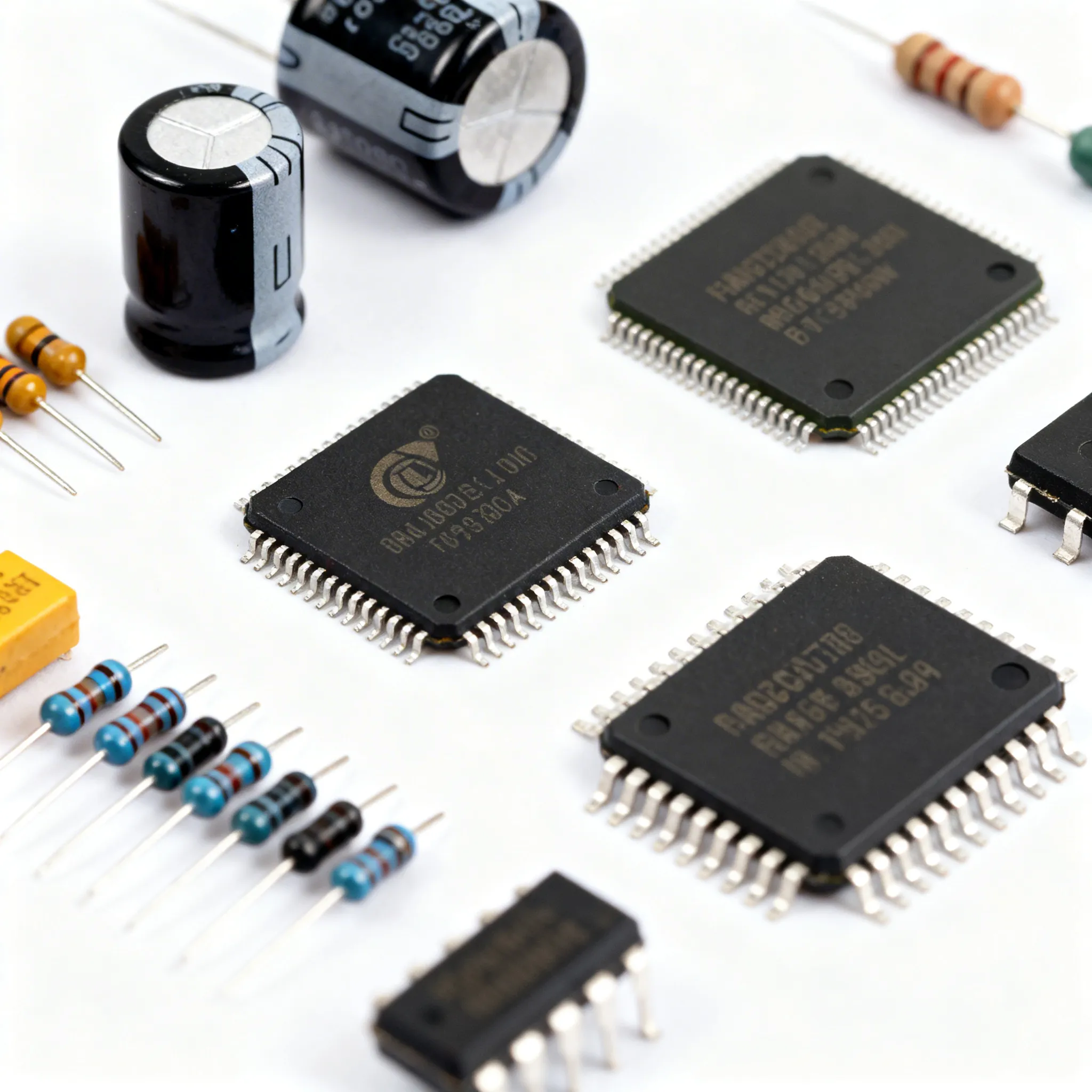
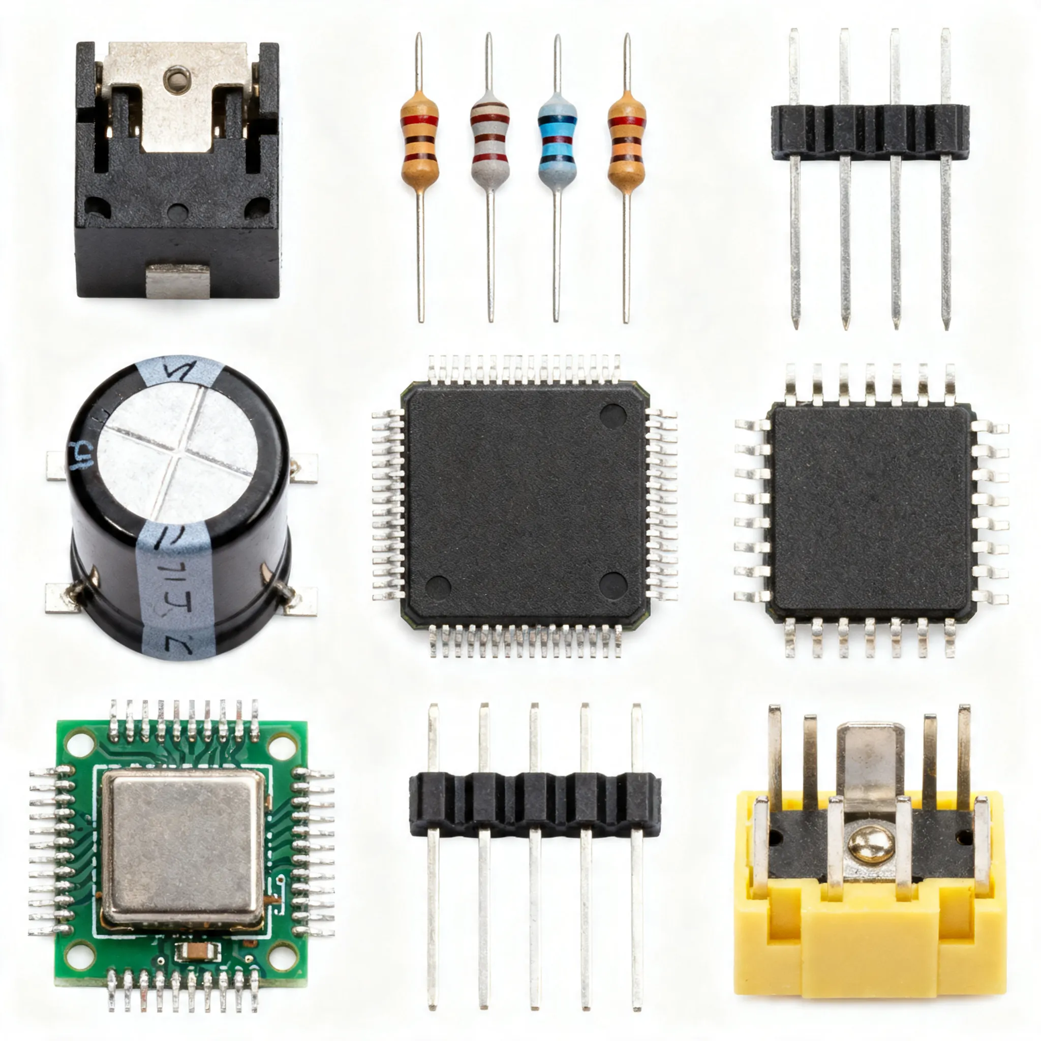
The Growing P-Channel MOSFET Market
The p-channel mosfet is not just a niche component; it is becoming a cornerstone of modern electronics. This shift is reflected in the strong growth of the p-channel mosfet market. The overall p-channel mosfet market is expanding significantly, with projections showing a Compound Annual Growth Rate (CAGR) of 5.6% from 2023 to 2030. This steady market growth signals that the technology is a reliable choice for future designs. The p-channel mosfet market is responding to a clear industry need for better power management.
Several key factors are driving the expansion of the p-channel mosfet market. The demand for high-performance power devices is rising across multiple sectors. Key market drivers include:
- Consumer Electronics: The constant innovation in smartphones, laptops, and wearable devices requires compact and energy-efficient power solutions. The p-channel mosfet is ideal for these applications.
- Internet of Things (IoT): The rise of IoT and Industry 4.0 technologies creates a massive need for efficient power control in sensors, robotics, and smart grid infrastructure.
- Automotive and Green Energy: The p-channel mosfet is also crucial in advanced automotive systems. Its role extends to managing power in electric vehicles and renewable energy systems.
At its core, the growth of the p-channel mosfet market is fueled by a universal demand for energy-saving components. As devices become smaller and more powerful, the need for high power density and superior efficiency makes the p-channel mosfet an essential semiconductor technology.
These trends confirm that the p-channel mosfet is a vital part of the future of advanced power semiconductor devices. The expanding p-channel mosfet market for low-voltage mosfets ensures that this mosfet technology will continue to evolve, offering even better performance for next-generation applications. The future of the p-channel mosfet market looks bright.
Why a P-Channel MOSFET Excels at High-Side Switching
Choosing the right component for power control is critical. A p-channel mosfet is often the best choice for a technique called high-side switching. This method places the mosfet between the positive power supply and the load. It acts like a gatekeeper, controlling the flow of power right from the source. This approach is fundamental to building energy-efficient devices.
The Basics of High-Side vs. Low-Side Control
Every electronic circuit needs a switch to control power. This switch can be placed in one of two positions. Low-side switching places the mosfet between the load and ground. High-side switching, conversely, places the mosfet between the power source and the load.
For battery-powered devices, high-side switching offers superior advantages. It completely disconnects the load from the power source. This action effectively eliminates standby current draw and prevents leakage. This method also provides significant safety and operational benefits.
- Enhanced Safety: It reduces the risk of a short circuit to the chassis ground, a common issue in systems with long cables.
- Built-in Protection: Modern high-side mosfets often include protection against over-voltage, under-voltage, and over-temperature conditions.
- Advanced Diagnostics: They can provide real-time feedback, allowing a microcontroller to detect faults like an open load or a short circuit.
Note: By cutting power at the source, high-side switching ensures the peripheral is truly "off." This is the most effective way to conserve energy and maximize battery life.
Why a P-Channel is Ideal for High-Side Switching
A p-channel mosfet is uniquely suited for high-side switching because of its simple gate control. A p-channel mosfet turns on when its gate voltage is pulled lower than its source voltage. Since the source is connected to the positive battery terminal, pulling the gate to ground (0V) creates the negative gate-source voltage (Vgs) needed to activate the mosfet.
This is much simpler than using an N-channel mosfet for the same task. An N-channel mosfet requires a gate voltage that is higher than its source voltage to turn on. When the source is already at the battery voltage, this becomes a problem. You would need a special circuit, like a charge pump or bootstrap driver, just to generate this higher voltage.
The p-channel mosfet eliminates this complexity entirely. A microcontroller's standard 3.3V or 5V logic pin can directly pull the gate low to turn the p-channel mosfet on and pull it high to turn it off.
| Feature | P-channel MOSFET (High-Side) | N-channel MOSFET (High-Side) |
|---|---|---|
| Gate Drive Voltage | Requires a negative Vgs (simple to achieve) | Requires a positive Vgs (complex to achieve) |
| Turn-on Condition | Gate is pulled to ground (0V) | Gate voltage must be higher than the source voltage |
| Circuit Complexity | Minimal; direct drive from a microcontroller | Requires a charge pump, bootstrap, or level-shifter circuit |
| Component Count | Low | High |
This direct compatibility makes the p-channel mosfet the clear winner for simple, efficient high-side load switching in battery-powered electronics.
How Simple Gate Drive Boosts Efficiency
The simplicity of a p-channel mosfet circuit directly translates to higher efficiency and lower power consumption. Fewer components mean a smaller board footprint and a lower bill of materials (BOM). More importantly, the simple gate drive circuit consumes very little power itself.
Complex gate drivers for N-channel mosfets are active circuits. They constantly consume power to maintain the higher gate voltage. A p-channel mosfet, however, can be controlled with a simple pull-up resistor. By choosing a high-value resistor (e.g., 100kΩ), the quiescent current needed to keep the mosfet off becomes incredibly small. This tiny current draw is a major factor in reducing overall power consumption, especially in devices that spend most of their time in standby mode. This design choice directly boosts battery life.
Implementing these power-saving designs correctly is key to unlocking their full potential. For complex system-on-chip (SoC) integrations, partnering with a solutions expert can accelerate development and ensure optimal performance. For instance, Nova Technology Company (HK) Limited is a HiSilicon-designated solutions partner specializing in advanced chip-level solutions. Collaborating with such partners helps engineering teams properly integrate p-channel mosfets and other power management ICs into sophisticated systems, ensuring maximum efficiency from the component level up to the final product. The right p-channel mosfet and design support lead to superior power efficiency.
Core Applications for Better Battery Life

The theory behind the p-channel mosfet is powerful. Its real value shines in practical applications. This component is a versatile tool for smart power control across many industries. From tiny wearables to large electric vehicles, the p-channel mosfet provides a simple path to efficient power management. Its ability to act as an ideal high-side switch makes it essential for modern electronics.
Load Switching in IoT and Wearables
Internet of Things (IoT) devices and wearables must operate for weeks, months, or even years on a single battery. This requires extremely low power consumption. Most of these devices spend their time in a deep sleep mode. They only wake up for brief moments to take a measurement or transmit data. A p-channel mosfet is perfect for this job.
Engineers use a p-channel mosfet to implement "power gating." The microcontroller can completely shut off power to power-hungry peripherals like Wi-Fi modules, GPS receivers, or complex sensors. When the peripheral is not needed, its power is cut at the source. This eliminates all standby and leakage currents from that part of the circuit.
A single p-channel mosfet acts as a simple, effective load switch. It allows a low-power microcontroller to control a high-current subsystem. This design is a cornerstone of achieving multi-year battery life in remote IoT applications.
This simple on/off control, driven directly from a microcontroller pin, is a key strategy. It ensures that power is only consumed when absolutely necessary, maximizing the device's operational life.
Key Applications for P-Channel MOSFETs
The use of the p-channel mosfet extends far beyond simple load switching. It is a fundamental component in a wide range of power management applications. Its reliability and efficiency make it a go-to choice for designers.
One of the most critical applications is in Battery Management Systems (BMS). These systems protect and manage rechargeable batteries. The p-channel mosfet helps control charging and discharging cycles safely. You can find this mosfet in:
- Consumer electronics like e-bike battery packs.
- Automotive systems, including the BMS for electric vehicles (EVs).
The p-channel mosfet is a workhorse in automotive electronics, appearing in systems like:
- Battery protection and reverse polarity protection circuits
- Infotainment systems and instrument clusters
- Advanced Driver Assistance System (ADAS) sensor modules
- Interior and exterior LED lighting controls
- Motor drives for seats and power steering
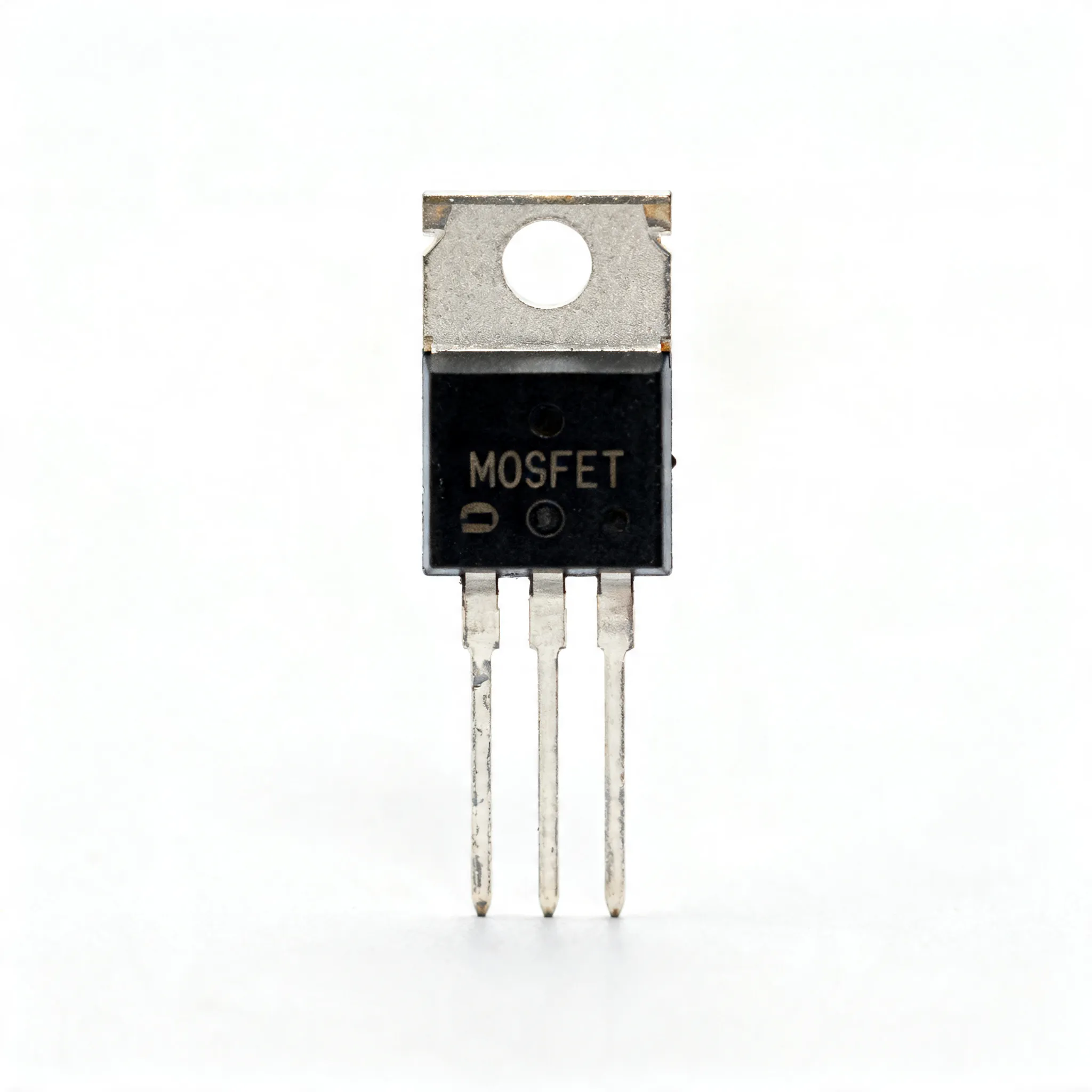
Another key use is reverse polarity protection. Accidentally connecting a battery backward can destroy a device. A p-channel mosfet offers a highly efficient solution. It blocks current flow if the polarity is reversed but allows it to pass with almost no voltage drop when connected correctly. Common mosfets for this task include the IRF9540 and Si2323.
Integrating these mosfets into complex systems requires expertise. For designs involving advanced System-on-Chips (SoCs), partnering with a specialist can ensure success. Nova Technology Company (HK) Limited, a HiSilicon-designated solutions partner, provides expert chip-level solutions. They help engineering teams properly integrate components like the p-channel mosfet into sophisticated power management schemes, ensuring maximum system efficiency.
Efficient Power Path Management
Many modern devices can be powered by multiple sources, such as an internal battery and an external USB charger. The system needs a way to seamlessly switch between them. A p-channel mosfet provides an elegant and efficient solution for this power path selection. This method is often used alongside DC/DC conversion circuits to supply a stable voltage.
Here is how a p-channel mosfet intelligently manages the power source:
- USB Power Connected: The USB provides 5V. This voltage is applied to both the source and the gate of the p-channel mosfet. The gate-to-source voltage (
Vgs) becomes 0V. A p-channel mosfet needs a negativeVgsto turn on, so it remains off. The system is powered directly by the USB. - USB Power Disconnected: The USB 5V disappears. A pull-down resistor pulls the mosfet's gate to ground (0V). The battery now provides voltage to the mosfet's source. This creates a negative
Vgs, which turns the p-channel mosfet on. - Battery Takes Over: Once the mosfet is on, it creates a low-resistance path. Power flows freely from the battery to the system. The switchover is automatic and smooth, with the mosfet's internal body diode helping to kickstart the process.
This automatic selection circuit is simple and consumes very little power. It prioritizes external power when available and ensures the battery is only used when needed. This is a prime example of efficient power management in action.
Selecting the Right MOSFET for Your Design
Choosing the right p-channel mosfet is crucial for an efficient design. Designers must balance several key parameters to maximize battery life and performance. Focusing on three specifications will guide you to the best p-channel mosfet for your application.
Low Rds(on) for Minimal Conduction Loss
The on-resistance, or Rds(on), is the resistance of the p-channel mosfet when it is fully turned on. This value is extremely important. A lower Rds(on) means less power is wasted as heat when current flows through the mosfet. This wasted power is called conduction loss.
- For high-current designs, a p-channel mosfet with a very low
Rds(on)is essential. - However, there is a trade-off. A mosfet with lower
Rds(on)often has a larger die size, which can increase gate charge and switching loss. - Remember that
Rds(on)also increases as the temperature of the mosfet rises.
Designers must balance Rds(on) with other factors. For low-frequency applications, minimizing Rds(on) is the top priority.
Logic-Level Vgs(th) for Direct Microcontroller Drive
The gate-source threshold voltage, or Vgs(th), is the minimum voltage needed to begin turning the p-channel mosfet on. For battery-powered devices, it is vital to select a "logic-level" p-channel mosfet. These mosfets are designed to be fully turned on by the low voltage signals from a microcontroller, typically 3.3V or 5V.
A logic-level p-channel mosfet simplifies your circuit. It allows a microcontroller to directly drive the mosfet gate without needing extra components. This reduces board space, lowers cost, and consumes less power.
Ensuring the Vgs(th) of the mosfet is compatible with your microcontroller's output voltage is a fundamental step for efficient power control.
Low Gate Charge (Qg) for Fast, Efficient Switching
Total Gate Charge, or Qg, is the amount of electrical charge needed to turn the mosfet on. This parameter directly controls the switching speed. A p-channel mosfet with a lower Qg can switch on and off much faster.
Faster switching reduces power loss that occurs during the transition from off to on. The relationship is simple: a lower gate charge allows for faster switching and higher efficiency. However, there is often a trade-off between Qg and Rds(on). A mosfet with a smaller chip size may have a low Qg but a higher Rds(on). For example, some p-channel mosfets designed for battery chargers have a Qg as low as 197 nC, enabling both fast switching and simple drive requirements. For high-frequency applications, choosing a p-channel mosfet with a low Qg is critical.
The p-channel mosfet is the superior choice for simple and effective high-side switching. Its use in battery-powered designs is a clear path to better power efficiency. The growing p-channel mosfet market confirms its importance. This p-channel mosfet reduces standby power draw and simplifies circuit design. The result is a significantly longer battery life for your device. Leading manufacturers like Littelfuse and ROHM Semiconductor offer a wide selection of p-channel mosfet options for load switching.
For your next battery-powered project, specify a p-channel mosfet for power management. This strategic choice will unlock maximum efficiency and performance. This p-channel mosfet is a powerful mosfet.
FAQ
Why is a P-channel better for high-side switching?
A P-channel MOSFET simplifies high-side switching. It turns on when its gate is pulled to ground, a simple task for a microcontroller. An N-channel MOSFET in the same position requires a complex, power-consuming circuit to generate a voltage higher than the power source.
What does Rds(on) mean for battery life?
Rds(on) is the MOSFET's resistance when it is on. A lower Rds(on) value means less power is wasted as heat. This reduction in wasted energy, known as conduction loss, directly translates to longer battery life, especially in high-current devices.
Can I control a P-channel MOSFET with a 3.3V microcontroller?
Yes, you can. You must select a "logic-level" P-channel MOSFET. These components are specifically designed to be fully activated by the low-voltage signals from a standard microcontroller. This allows for direct control without extra parts, saving space and power.
When is low gate charge (Qg) important?
Low gate charge (Qg) is crucial for high-frequency applications. A lower Qg allows the MOSFET to switch on and off faster. This speed reduces switching losses, which is the power wasted during transitions. This makes the entire system more efficient.