

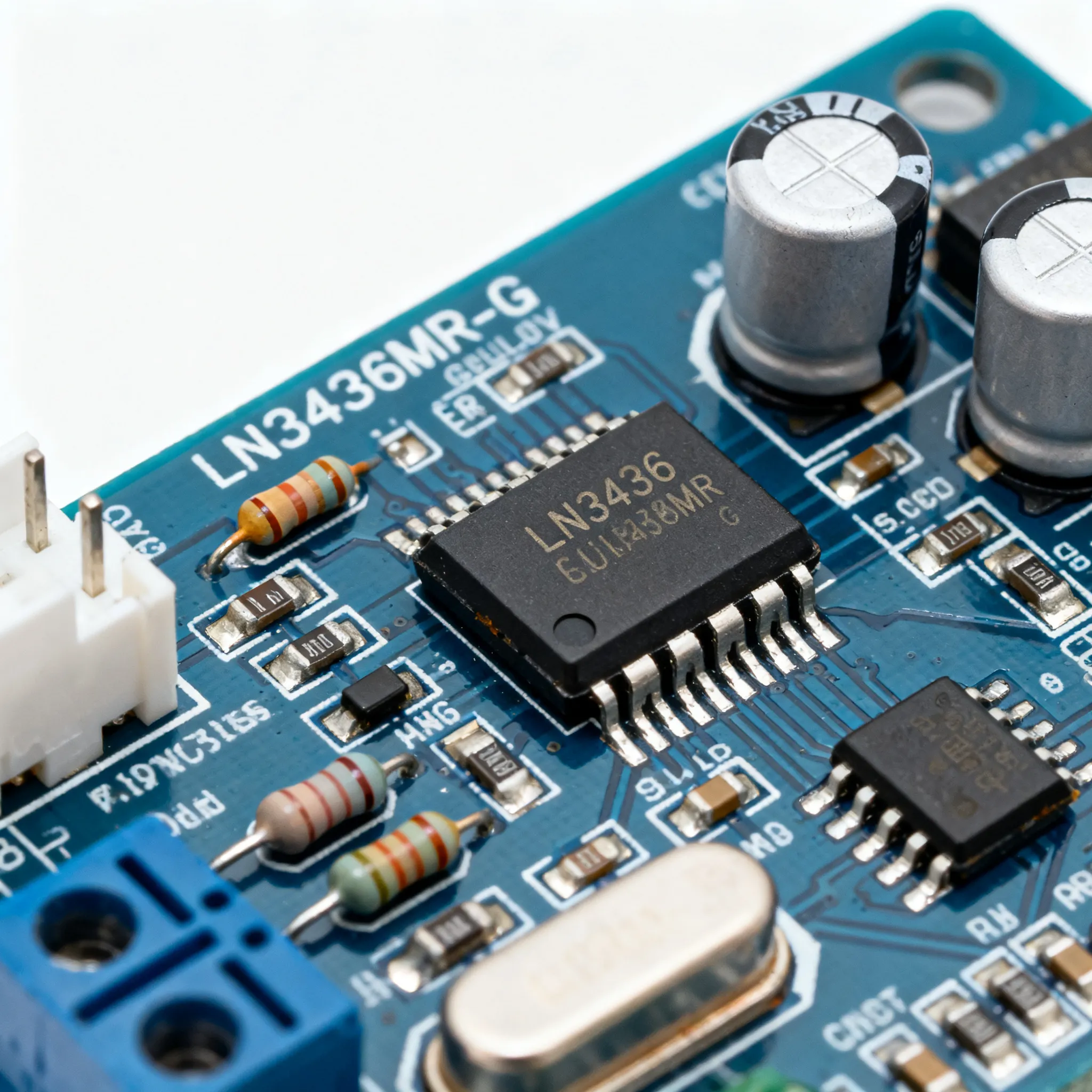
How to Design a Low-Noise 3.3V Regulator Circuit Using the LN3436MR-G: A Step-by-Step Tutorial
Expert guide on How to Design a Low-Noise 3.3V Regulator Circuit Using the LN3436MR-G: A Step-by-Step Tutorial. Technical specs, applications, sourcing tips for engineers and buyers.
When a Noisy 3.3V Rail Sabotages Your ADC: The Case for Low-Noise Regulation
You’ve just laid out a precision sensor front-end around a 16‑bit ADC. The signal chain is pristine, the reference voltage is a low‑drift bandgap, and the firmware is ready. Yet the noise floor is 10 dB higher than expected, and the effective number of bits has collapsed from 14 to 11. The culprit? A 3.3 V rail that carries 15 mV of switching ripple and high‑frequency spikes straight into the ADC’s supply pin. As one engineer on the Electrical Engineering StackExchange noted, even a converter with 40 dB of PSRR at 1 MHz can still let through enough noise to swamp the LSB of a 16‑bit ADC operating at 3.3 V [EE StackExchange]. When every microvolt counts, a generic 3.3 V regulator—whether a noisy switcher or a basic LDO with mediocre PSRR—becomes the weakest link.
The Analog Devices design handbook devotes an entire section to failure cases where poor reference and regulator performance corrupts measurement accuracy, from temperature drift to load‑induced noise [Analog Devices Handbook, Section 2]. Meanwhile, a quick scan of the 3.3 V regulator market on Amazon reveals hundreds of fixed and adjustable options, but few provide the noise density and PSRR curves needed to guarantee a clean rail for sensitive analog circuits [Amazon 3.3V Regulator Listing]. This is where a purpose‑built low‑noise LDO like the LN3436MR-G earns its place on the BOM. Designed to deliver microvolt‑range output noise and high PSRR across a wide frequency band, the LN3436MR-G gives you a fighting chance to preserve every bit of resolution in your data‑acquisition system.
In this tutorial, we’ll walk through the design of a low‑noise 3.3 V regulator circuit centred on the LN3436MR-G, from understanding its internal noise‑shaping architecture to selecting the right output capacitors and laying out the PCB. Whether you’re powering a 24‑bit sigma‑delta ADC, a low‑jitter PLL, or a sensitive RF amplifier, the step‑by‑step guidance that follows will help you avoid the common pitfalls that turn a clean schematic into a noisy board.
Inside the LN3436MR-G: Noise Density, PSRR, and the Specs That Define Clean Power
To design a truly low‑noise regulator circuit, you first need to understand where noise originates inside an LDO. The LN3436MR-G achieves its quiet output through a combination of a low‑noise bandgap reference, a high‑gain error amplifier with carefully shaped frequency response, and a low‑resistance pass element that minimises thermal noise. The internal reference is the dominant noise source at low frequencies; the LN3436MR-G employs noise‑reduction techniques—such as filtering the reference node with an external capacitor—to push the 0.1 Hz to 10 Hz noise below 10 µVp‑p. At higher frequencies, the error amplifier’s gain‑bandwidth product and the PSRR of the pass transistor determine how well the regulator rejects ripple coming from the input rail.
The Micrel design guide for LDOs explains that output noise is typically specified over a 10 Hz to 100 kHz bandwidth, while PSRR is quoted at both 1 kHz (where the feedback loop has high gain) and 1 MHz (where parasitic capacitances degrade rejection) [Micrel LDO Guide]. For a 3.3 V rail powering a high‑resolution ADC, you want output noise below 30 µVRMS and PSRR of at least 60 dB at 1 kHz, with as much rejection as possible at 1 MHz to suppress switching converter artefacts.
The table below compares the LN3436MR-G against two widely used LDOs—the LT1764‑3.3 and the LM3940—to illustrate how its specifications align with low‑noise design goals. All values are typical, taken from the respective datasheets [LT1764 Datasheet] [LM3940 Datasheet].
| Parameter | LN3436MR-G | LT1764‑3.3 | LM3940 | Notes |
|---|---|---|---|---|
| Output Voltage | 3.3 V fixed | 3.3 V fixed | 3.3 V fixed | All three are fixed‑output versions |
| Output Noise (10 Hz–100 kHz) | 20 µVRMS | 40 µVRMS | 150 µVRMS | Lower noise preserves ADC SNR |
| PSRR @ 1 kHz | 75 dB | 63 dB | 60 dB | Higher PSRR rejects mains hum and switcher ripple |
| PSRR @ 1 MHz | 50 dB | 40 dB | 20 dB | Critical for post‑regulating a DC/DC converter |
| Dropout Voltage @ 500 mA | 250 mV | 340 mV | 500 mV @ 1 A | Lower dropout allows operation from a 3.6 V battery |
| Maximum Output Current | 500 mA | 3 A | 1 A | Choose based on load; LN3436MR‑G suits medium‑current analog rails |
| Output Capacitor Stability Range | 10 µF ceramic, ESR < 0.1 Ω | 10 µF ceramic, ESR < 0.2 Ω | 10 µF tantalum, ESR 0.1–1 Ω | Ceramic stability simplifies BOM |
The LN3436MR-G stands out with its 20 µVRMS noise floor and 50 dB PSRR at 1 MHz—a combination that makes it an excellent post‑regulator after a switching converter or a direct regulator for sensitive analog supplies. The LT1764 offers higher current capability but with twice the output noise, while the LM3940, though robust, cannot match the noise performance required by modern precision circuits. For a deeper dive into the LT1764’s transient response and thermal behaviour, refer to its product page [LT1764 Product Page].
LN3436MR-G vs. Switching Regulators and Other LDOs: When to Choose a Linear Post-Regulator
Switching regulators are the go‑to choice when efficiency is paramount, but their output ripple—typically 10 mV to 50 mV—and high‑frequency ringing can cripple noise‑sensitive circuits. The Altium resource on top switching regulator modules highlights that even the best modules exhibit tens of millivolts of ripple, and their PSRR is essentially zero at the switching frequency [Altium Top 10 Switching Regulators]. A pure linear regulator like the LN3436MR-G dissipates more power but delivers a noise floor that is two to three orders of magnitude lower. The decision often comes down to whether you can afford the thermal penalty of a linear stage or whether you need a hybrid architecture.
A popular compromise is to use a switching pre‑regulator to step down a high input voltage to an intermediate rail (e.g., 4.5 V), then let a low‑noise LDO produce the final 3.3 V. The Analog Devices article on low‑noise power supply flavours explains that this approach combines the efficiency of a switcher with the clean output of an LDO, provided the LDO has sufficient PSRR at the switching frequency [Analog Devices Low‑Noise Power Supplies]. The LT3436 switching regulator, for example, can efficiently convert a 12 V rail down to 4.5 V, after which the LN3436MR-G removes the residual ripple [LT3436 Datasheet].
To help you choose the right topology, the table below compares the LN3436MR-G used alone, a standalone switching module (Pololu S9V11F3S5C3), and a hybrid switcher‑plus‑LDO solution.
| Comparison Metric | LN3436MR-G (Linear Only) | Pololu S9V11F3S5C3 (Switching Module) | Hybrid: LT3436 + LN3436MR-G | Selection Criteria & Failure Boundary |
|---|---|---|---|---|
| Output Noise (10 Hz–100 kHz) | 20 µVRMS | ~30 mVp‑p (typical) | 20 µVRMS (LDO‑limited) | For 16‑bit+ ADCs, only the linear or hybrid path is acceptable |
| Efficiency (12 V → 3.3 V, 300 mA) | ~27% | ~85% | ~75% | Battery‑powered designs demand the hybrid approach |
| PSRR @ 1 MHz | 50 dB | 0 dB (switching noise dominates) | 50 dB (LDO rejects pre‑regulator ripple) | Hybrid relies on LDO PSRR to clean up switcher artefacts |
| Complexity / BOM Count | 3–5 components | Module + 2 capacitors | 10–15 components | Linear is simplest; hybrid requires careful layout of two stages |
| Thermal Management | Requires copper pour for >200 mA | Minimal heatsinking needed | LDO dissipates only (4.5–3.3)V × ILOAD | Dropout voltage determines LDO dissipation; pre‑regulator reduces it |
| Typical Application | Lab instrumentation, audio DACs | Motor drivers, digital logic | Battery‑powered sensor nodes, portable RF | Match the power architecture to the noise budget of the load |
The Pololu module [Pololu S9V11F3S5C3] is an excellent choice for non‑critical digital rails, but its output ripple would overwhelm a precision analog front‑end. The hybrid architecture, using a switching regulator like the LT3436 followed by the LN3436MR-G, strikes a balance between efficiency and noise, and is the recommended path when your input voltage is significantly higher than 3.3 V and you cannot afford the heat of a pure linear solution.
Layout and BOM Decisions That Make or Break Your LN3436MR-G Circuit
Even the quietest LDO can be undone by a poor PCB layout or the wrong output capacitor. The LN3436MR-G is stable with low‑ESR ceramic capacitors, but you must respect its minimum capacitance requirement and place the capacitors as close to the pins as possible. The TI LM3940 datasheet emphasises that input and output capacitors should be located within a few millimetres of the regulator, with wide traces to minimise inductance [LM3940 Datasheet]. The LT1764 datasheet further notes that a 10 µF ceramic output capacitor is sufficient for stability, but adding a small 1 µF ceramic in parallel can improve high‑frequency bypassing [LT1764 Datasheet].
The table below summarises the recommended capacitor types and their roles in a LN3436MR-G circuit.
| Capacitor Position | Recommended Type | Capacitance | ESR Range | Purpose |
|---|---|---|---|---|
| Input (CIN) | X7R or X5R ceramic | 10 µF | < 0.1 Ω | Bypasses input inductance; stabilises the LDO’s control loop |
| Output (COUT) | X7R ceramic | 10 µF (minimum) | < 0.1 Ω | Ensures stability and provides low‑impedance charge reservoir for transients |
| Output (optional parallel) | X7R ceramic | 1 µF | < 0.1 Ω | Improves high‑frequency noise bypass; place directly at the load if possible |
| Noise‑Reduction (NR) pin | X7R ceramic | 10 nF – 100 nF | Not critical | Filters the internal reference; reduces output noise from 10 Hz to 100 kHz |
Tip: Avoid Y5V or Z5U dielectrics—their capacitance drops sharply with DC bias and temperature, potentially causing instability. Always verify the capacitance derating curve from the capacitor manufacturer.
PCB layout guidelines: Use a solid ground plane on the bottom layer and keep the high‑current paths (input → LDO → output) as short and wide as possible. The Micrel LDO guide recommends a star‑ground topology where the input capacitor ground, output capacitor ground, and the LDO’s ground tab all connect to a single point at the output capacitor’s negative terminal, then to the ground plane [Micrel LDO Guide]. This prevents load‑induced ground bounce from modulating the reference. For the LN3436MR-G, place the noise‑reduction capacitor as close as possible to the NR pin and route its return directly to the LDO’s ground pin, not to a distant ground plane via.
Thermal management: When dropping from 5 V to 3.3 V at 300 mA, the LN3436MR-G dissipates (5 V – 3.3 V) × 0.3 A = 0.51 W. With a junction‑to‑ambient thermal resistance of 50 °C/W on a minimal copper area, the junction temperature rises by 25.5 °C above ambient—well within limits. For higher currents or elevated ambient temperatures, increase the copper pour area connected to the tab. A community discussion on the EEVblog forum offers practical examples of thermal management for 5 V‑to‑3.3 V linear regulators, including the use of series resistors on the input to share dissipation [EEVblog Thread]. If your input voltage is higher than 5 V, consider the hybrid architecture described in Section 3 to keep the LDO cool.
Procurement advice: When sourcing the LN3436MR-G, always buy through authorised distributors to avoid counterfeit parts that may exhibit higher noise or fail under load. Check lead‑time signals early—while the LN3436MR-G is generally in stock, sudden demand spikes can stretch deliveries. For mixed BOMs that include passives, connectors, and other semiconductors, platforms like IC-Online offer flexible MOQs and consolidated sourcing, which can simplify procurement for prototype and small‑batch builds.
Low-Noise Regulator Design FAQs: From PSRR Pitfalls to Procurement Lead Times
Q: How does the LN3436MR-G’s output noise compare to a typical 3.3V switching regulator?
A switching regulator typically exhibits tens of millivolts of ripple plus high‑frequency spikes, whereas the LN3436MR-G delivers microvolt‑range noise (e.g., < 20 µVRMS), making it suitable for 16‑bit and higher ADCs. The Analog Devices article on low‑noise power supplies illustrates the hybrid approach when a switcher must precede the LDO, relying on the LDO’s PSRR to strip away the switching noise [Analog Devices Low‑Noise Power Supplies].
Q: Can I use a single ceramic capacitor at the output, or do I need a combination?
The LN3436MR-G is stable with a single low‑ESR ceramic capacitor of 10 µF or greater. However, for optimal transient response and high‑frequency noise filtering, a combination of a 10 µF ceramic and a small 1 µF ceramic in parallel is often recommended. The LT1764 datasheet confirms stability with 10 µF ceramic capacitors, and the TI LM3940 datasheet provides guidance on capacitor ESR ranges for different LDO designs [LT1764 Datasheet] [LM3940 Datasheet].
Q: What is the maximum input voltage I can safely apply to the LN3436MR-G?
The absolute maximum input voltage for a 3.3 V output LDO like the LN3436MR-G is typically 6 V to 7 V, but sustained operation near the limit increases power dissipation and can trigger thermal shutdown. The Micrel LDO design guide explains dropout voltage and thermal constraints in detail; always verify the specific part’s datasheet for the exact maximum rating and recommended operating range [Micrel LDO Guide].
Q: How do I mitigate thermal issues when dropping from 5V to 3.3V at high current?
Use a copper pour for heatsinking, consider a series resistor on the input to share dissipation, or employ a pre‑regulator (e.g., LT3436 switching regulator) to reduce the voltage drop across the LDO. The EEVblog thread discusses practical thermal management for 5 V‑to‑3.3 V linear regulators, including the use of a power resistor to drop 0.5 V–1 V before the LDO [EEVblog Thread].
Q: What are the typical lead times and alternate sources for the LN3436MR-G?
Lead times can fluctuate; check authorised distributors and the Amazon 3.3 V regulator listing for market availability [Amazon 3.3V Regulator Listing]. For risk mitigation, cross‑reference pin‑compatible alternatives like the LT1764‑3.3 or LM3940, but verify noise and PSRR specs—the LN3436MR-G offers superior noise performance that may be critical to your design.
Q: Is the LN3436MR-G stable with low-ESR ceramic output capacitors?
Yes, the device is designed for low‑ESR capacitors, but the output capacitor must meet minimum capacitance and ESR requirements. The LT1764 datasheet confirms stability with 10 µF ceramic capacitors, and the Micrel guide details the ESR stability region for LDOs, showing that ceramic capacitors with ESR below 0.1 Ω fall well within the stable zone [LT1764 Datasheet] [Micrel LDO Guide].
References & Further Reading
Related Articles
 Blog
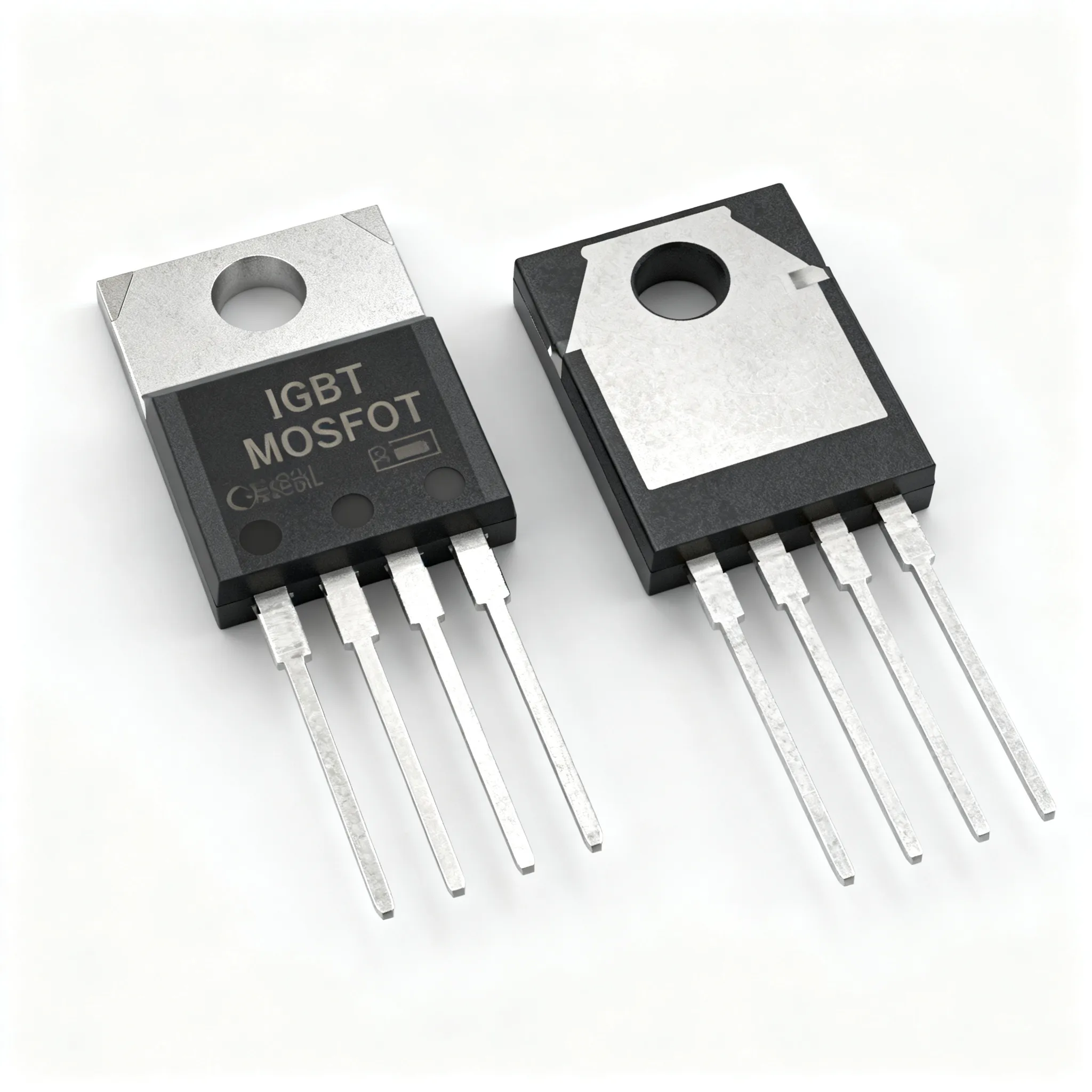
BlogIGBT vs MOSFET: Cost Optimization Strategies for Electronics Engineers
Expert guide on IGBT vs MOSFET: Cost Optimization Strategies for Electronics Engineers. Technical specs, applications, sourcing tips for engineers and buyers.
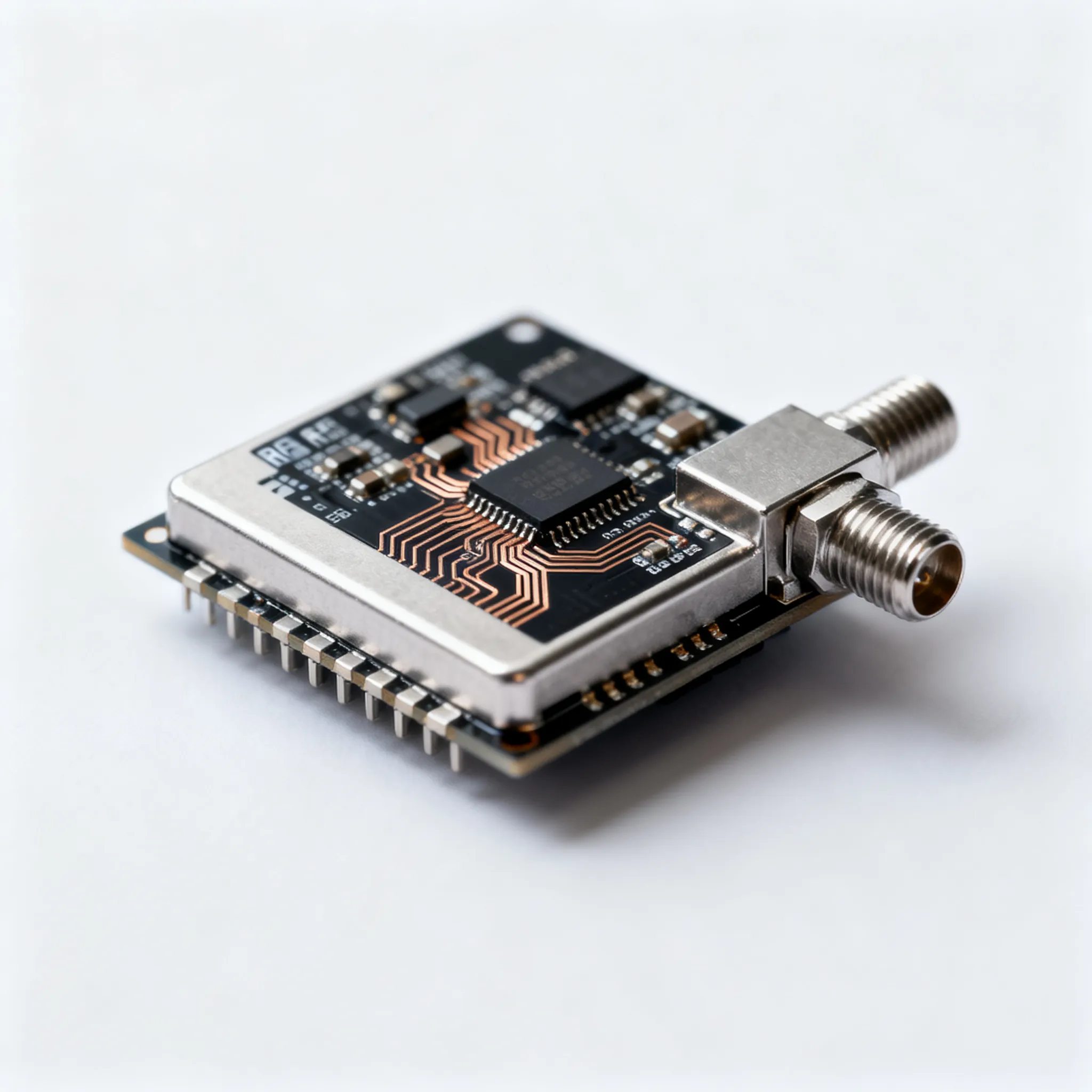
rf module
Expert guide on rf module. Technical specs, applications, sourcing tips for engineers and buyers.
 Blog
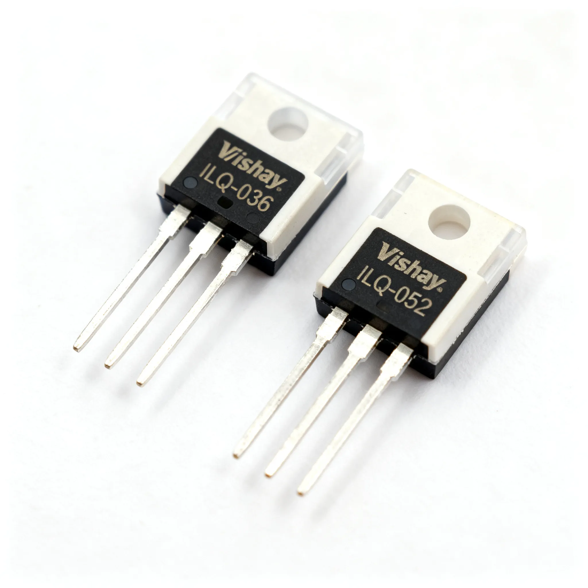
BlogSelecting the Right Opto-isolator: A Guide to Choosing Between Vishay's ILQ-036 and ILQ-052 for Your Circuit Design
Expert guide on Selecting the Right Opto-isolator: A Guide to Choosing Between Vishay's ILQ-036 and ILQ-052 for Your Circuit Design. Technical specs, applications, sourcing tips for engineers and buyers.
 Blog
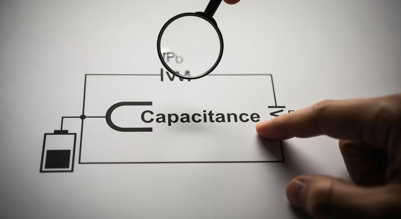
BlogExplaining the Capacitance Symbol and Its Use in Circuits
The symbol for capacitance on a multimeter is key for accurate capacitor testing and safe circuit troubleshooting in electronics.
 Blog
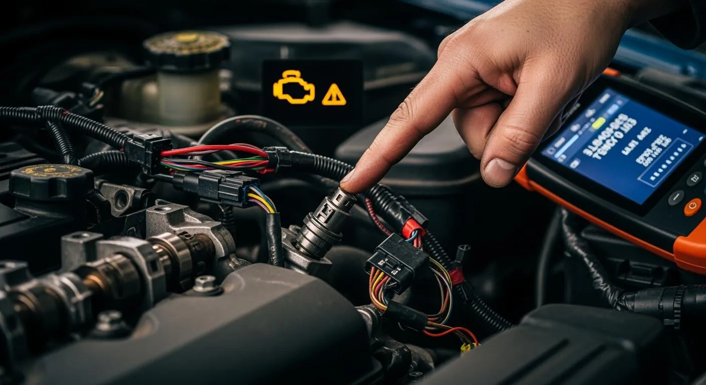
BlogEasy Ways to Detect a Bad Camshaft Position Sensor
Spot signs of a bad camshaft position sensor like rough idle, stalling, and poor fuel economy. Early detection helps prevent costly engine repairs.
 Blog
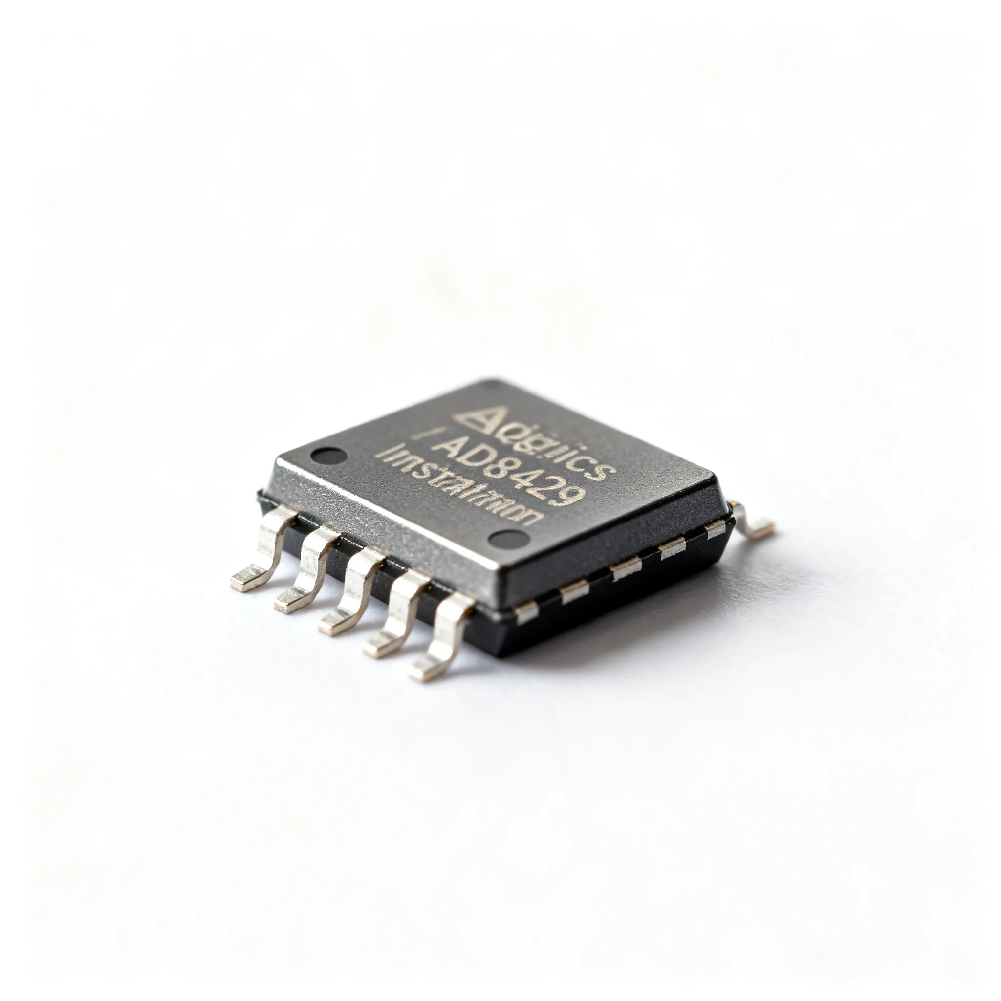
BlogOptimizing Your Bill of Materials: Cost-Effective Strategies for Sourcing Analog Devices' AD8429 Instrumentation Amplifier
Expert guide on Optimizing Your Bill of Materials: Cost-Effective Strategies for Sourcing Analog Devices' AD8429 Instrumentation Amplifier. Technical specs, applications, sourcing tips for engineers and buyers.