SD24C-01FTG TVS Diode Selection Guide: Protecting High-Speed Data Lines
Expert guide on SD24C-01FTG TVS Diode Selection Guide: Protecting High-Speed Data Lines. Technical specs, applications, sourcing tips for engineers and buyers.
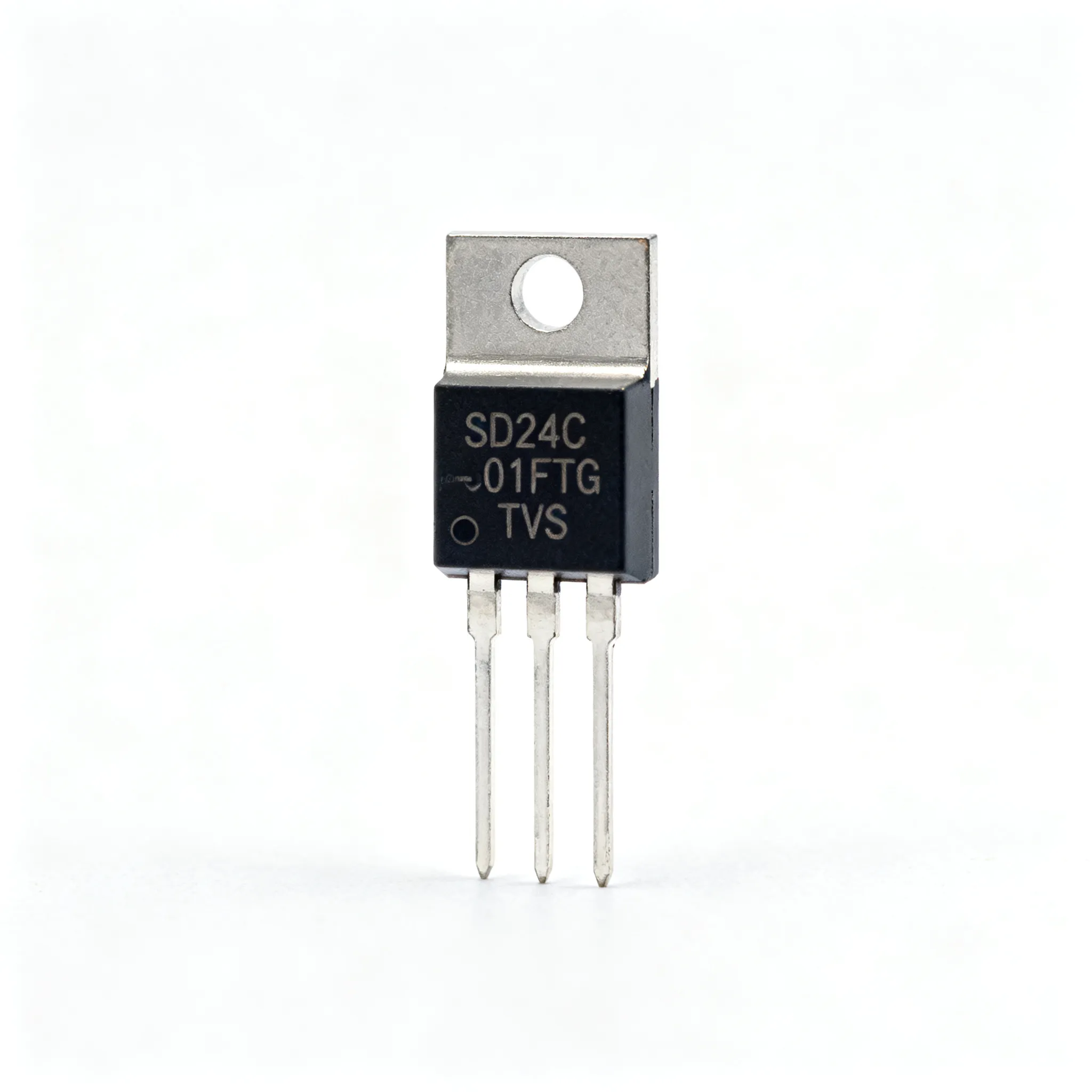
Why High-Speed Data Lines Can’t Afford a Generic TVS Diode
When your differential pair is pushing 20 Gbps NRZ through a USB4 or HDMI 2.1 interface, every fraction of a picofarad counts. A generic 24 V TVS diode might promise solid ESD protection, but its 10–50 pF junction capacitance will load the line, round the edges of your eye diagram, and introduce bit errors that no amount of receiver equalization can fix. As recent EE Times analysis of high-speed design emphasizes, signal integrity at multi-gigabit rates is a game of picoseconds and millivolts—and a poorly chosen protection device can collapse the eye before the signal even reaches the connector.
Engineers who have spent time debugging intermittent link drops on USB 3.2 or Thunderbolt 4 know the pattern: the system passes ESD testing but fails in the field because the TVS capacitance, combined with trace stubs and connector parasitics, pushes the channel beyond its loss budget. The SD24C-01FTG was designed specifically to break this compromise. With a typical capacitance of just 0.5 pF and a 24 V stand-off voltage, it gives you the headroom to protect higher-voltage data lines—like 20 V USB Power Delivery VBUS sense lines, RS-485 transceivers, or industrial sensor interfaces—without sacrificing the signal quality that modern SerDes blocks demand.
This selection guide walks you through the electrical fundamentals, compares the SD24C-01FTG against other low-cap TVS options, and delivers practical layout and sourcing advice. Whether you are an SI engineer fine-tuning a channel simulation or a procurement buyer qualifying a second source, the goal is the same: pick a TVS that protects the silicon without killing the signal.
How the SD24C-01FTG Delivers ESD Protection Without Killing Your Signal
At its core, the SD24C-01FTG is a single-channel, bidirectional TVS diode built on a low-capacitance process. The device’s 24 V reverse stand-off voltage (VRWM) means it remains essentially off during normal operation, drawing negligible leakage current even when the line voltage sits at 20 V DC—a common scenario in USB PD 3.1 systems or 24 V-tolerant industrial I/O. When an ESD strike hits, the internal snap-back structure triggers within nanoseconds, shunting the transient current to ground while clamping the voltage to a safe level for the downstream ASIC or PHY.
What sets the SD24C-01FTG apart from a generic 24 V TVS array is its junction capacitance. A standard 600 W TVS in an SMA package might exhibit 50 pF at 0 V bias; even a smaller SOT-23 device often lands in the 10–30 pF range. The SD24C-01FTG squeezes that down to 0.5 pF typical (1 pF maximum) by using a proprietary low-cap architecture—likely a steering diode bridge with a central Zener clamp, though the exact die topology is proprietary. The result is an insertion loss at 10 GHz that stays below -0.5 dB, keeping the differential return loss well within the -15 dB mask that most high-speed standards require.
Key Takeaway: The diode’s ultra-low capacitance is not a marketing number; it directly determines whether your 10 Gbps eye diagram stays open or collapses into a closed blob. At 0.5 pF, the capacitive loading is roughly equivalent to a few millimeters of microstrip trace—manageable with careful layout.
Electrical Characteristics at a Glance
The table below compares the SD24C-01FTG against a typical off-the-shelf 24 V TVS diode in a comparable package. The differences in capacitance and clamping voltage explain why the SD24C-01FTG is the preferred choice for high-speed data lines.
| Parameter | SD24C-01FTG | Generic 24 V TVS (SOD-323) | Unit/Notes |
|---|---|---|---|
| Reverse Stand-off Voltage (VRWM) | 24 | 24 | V |
| Breakdown Voltage (VBR) min | 26.7 | 26.7 | V |
| Clamping Voltage (VC) @ 8 kV contact (IEC 61000-4-2) | < 15 | 40–60 | V; measured at device terminals |
| Typical Junction Capacitance @ 0 V, 1 MHz | 0.5 | 25 | pF |
| Maximum Junction Capacitance | 1.0 | 50 | pF |
| ESD Rating (IEC 61000-4-2 Contact) | ±30 kV | ±30 kV | kV |
| Peak Pulse Power (8/20 µs) | 350 | 600 | W |
| Package | DFN1006-2L (1.0×0.6×0.5 mm) | SOD-323 (1.7×1.25×0.95 mm) | mm |
| Operating Temperature Range | -55 to +125 | -55 to +150 | °C |
Notice the clamping voltage difference: while both devices carry a ±30 kV ESD rating, the SD24C-01FTG clamps at under 15 V during an 8 kV contact discharge, whereas the generic part lets the voltage spike to 40–60 V. That 40 V surge can easily punch through the gate oxide of a 28 nm or 16 nm FinFET transceiver. The low clamping voltage is a direct consequence of the diode’s fast turn-on and low dynamic resistance—characteristics that become critical when protecting sensitive 1.8 V or 3.3 V I/O rails on the same chip.
Equally important is the package. The DFN1006-2L (also called SOD-882) measures just 1.0 mm × 0.6 mm, with a 0.5 mm height. This tiny footprint reduces parasitic lead inductance to less than 0.5 nH, which helps keep the clamping voltage low and minimizes the loop area for the ESD current return path. When you place this part right at the connector, the ground via can be less than 1 mm away, creating a tight, low-impedance path to the chassis or board ground plane.
SD24C-01FTG vs. Alternative Low-Cap TVS Diodes: A Head-to-Head Look
No component selection happens in a vacuum. Engineers often evaluate other single-channel, low-capacitance TVS diodes to see if they can achieve similar protection with a different part—perhaps one that is already on the approved vendor list or available at a preferred distributor. The table below pits the SD24C-01FTG against two credible alternatives that also target high-speed interfaces: the Nexperia PESD24VS1UA and the ON Semiconductor ESD9B24.0ST5G. Both are 24 V stand-off devices with low capacitance, but the nuances matter.
| Comparison Metric | SD24C-01FTG | Nexperia PESD24VS1UA | ON Semi ESD9B24.0ST5G | Selection Criteria & Failure Boundary |
|---|---|---|---|---|
| Stand-off Voltage (VRWM) | 24 V | 24 V | 24 V | All three meet the 24 V requirement for USB PD and RS-485. |
| Typical Capacitance @ 0 V | 0.5 pF | 1 pF | 0.5 pF | At 20 Gbps, 0.5 pF vs 1 pF can mean 2–3 dB more insertion loss; the SD24C-01FTG and ESD9B24.0ST5G have the edge. |
| Clamping Voltage @ 8 kV Contact (typ) | < 15 V | ~20 V | ~18 V | Lower is always better for 3.3 V and 1.8 V PHYs; the SD24C-01FTG offers the lowest clamping of the group. |
| ESD Rating (IEC 61000-4-2 Contact) | ±30 kV | ±30 kV | ±30 kV | All exceed the typical 8 kV system requirement; headroom is comparable. |
| Package (mm) | DFN1006-2L (1.0×0.6) | SOD-882 (1.0×0.6) | SOD-923 (0.8×0.6) | Footprint differences are minimal; all are suitable for high-density layouts. SOD-923 is slightly smaller but may require tighter assembly tolerances. |
| Dynamic Resistance (RDYN) | ~0.3 Ω | ~0.5 Ω | ~0.4 Ω | Lower RDYN translates directly to lower clamping voltage at high peak currents; the SD24C-01FTG leads. |
| Availability / Second Source Risk | Single source (ProTek Devices) | Broadly available from Nexperia | Broadly available from ON Semi | If a drop-in replacement is mandatory, the SD24C-01FTG is unique; buffer stock or approved alternates should be qualified for risk mitigation. |
What the table reveals is that the SD24C-01FTG sits in a sweet spot: it matches the lowest capacitance of the group while delivering the lowest clamping voltage. The Nexperia PESD24VS1UA, while an excellent part with wide distribution, carries twice the capacitance—a penalty that may force you to shorten trace lengths or add re-timers. The ON Semi ESD9B24.0ST5G comes close on capacitance but still clamps a few volts higher. For a USB 3.2 Gen 2×2 link where the PHY operates at 1.2 V, those extra volts can be the difference between a clean bit stream and a CRC error storm.
Note: If your application does not require a 24 V stand-off—say you are protecting a 5 V HDMI TMDS line—then a 5 V device like the Semtech RClamp0524P (0.5 pF, 5 V) may be a better fit because its lower stand-off voltage yields an even lower clamping voltage. But for 24 V-tolerant interfaces, the SD24C-01FTG remains the primary option that doesn’t force you to compromise on capacitance.
From Spec to Layout: Practical Selection and Sourcing Tips for the SD24C-01FTG
Selecting the right TVS diode on paper is only half the battle. The difference between a robust design and a field failure often comes down to PCB layout and supply-chain discipline. The SD24C-01FTG’s 0.5 pF capacitance and 24 V stand-off open up a range of applications, but each interface imposes its own constraints.
Matching the 24 V Stand-off to Real Interfaces
The 24 V reverse stand-off voltage is not a random number. It aligns perfectly with several common industrial and consumer interfaces:
- USB Power Delivery (PD) 3.1: VBUS can reach 20 V, and the CC/SBU lines may see up to 21 V during cable discovery. A 24 V TVS provides a safe margin without clamping during normal operation.
- RS-485 / RS-422: Many transceivers operate with a common-mode voltage range of -7 V to +12 V, but industrial environments often require 24 V tolerance for fault conditions. The SD24C-01FTG protects the bus pins without interfering with the differential signal.
- Industrial Sensor Interfaces (IO-Link, 4–20 mA): 24 V is the de facto supply voltage in factory automation. Placing the SD24C-01FTG on the data line guards against ESD and surge transients while keeping the capacitive load negligible for the relatively low data rates (typically 230.4 kbps for IO-Link, but the low capacitance still helps avoid signal distortion on long cables).
Layout Rules That Keep the Clamping Voltage Low
Even the best TVS diode cannot protect your circuit if the layout adds inductance. Every millimeter of trace between the connector pin and the TVS, or between the TVS and the ground plane, adds about 0.5–1 nH of inductance. During an 8 kV ESD strike, the current rise time can be less than 1 ns, so a mere 1 nH of inductance generates a voltage spike of V = L × dI/dt ≈ 1 nH × (30 A / 1 ns) = 30 V—on top of the diode’s clamping voltage. The protected IC then sees 45 V instead of 15 V, potentially causing damage.
To avoid this, follow these layout guidelines, which align with the workmanship standards described in IPC-A-610 for SMD assembly:
- Place the TVS as close as possible to the connector or the point of entry. For a USB-C receptacle, the SD24C-01FTG should sit within 2 mm of the pin it protects.
- Route the protected trace through the TVS pad first, then to the IC. Do not create a stub; the signal should flow from connector → TVS pad → series element (if any) → IC.
- Use a direct via to the ground plane directly under the TVS’s ground pad. The via should be as large as practical (0.3–0.5 mm diameter) and placed immediately adjacent to the pad. Multiple vias are even better.
- Keep the ground plane solid and uninterrupted under the ESD current path. Avoid splits or neck-downs that would force the return current to take a longer path.
The table below summarizes the critical layout parameters and their impact on real-world clamping performance.
| Layout Parameter | Recommended Value | Impact on Clamping Voltage |
|---|---|---|
| Distance from connector pin to TVS pad | < 2 mm | Each extra mm adds ~1 nH, increasing peak voltage by ~30 V during an 8 kV strike. |
| Trace width between TVS and protected IC | Match 50 Ω / 90 Ω differential impedance | Impedance discontinuities cause reflections that can worsen the eye diagram, especially above 5 Gbps. |
| Ground via count and placement | At least 2 vias, directly under the TVS GND pad | Reduces ground inductance, lowering the residual voltage seen by the IC. |
| Stub length on protected line | 0 mm (route through pad) | A stub acts as a capacitive load and an antenna; even 1 mm can degrade return loss at 10 GHz. |
| Distance from TVS to any series capacitor/ESD choke | TVS must be on the connector side of any series element | Placing the TVS after a series component allows the transient to reach the IC before the TVS clamps. |
Sourcing and Supply-Chain Considerations
From a procurement perspective, the SD24C-01FTG is a single-sourced component, which means your BOM risk management should account for potential allocation or lead-time swings. Authorized distributors typically carry the part on 3,000- or 5,000-piece reels, and sample quantities are available for prototyping. Lead times have historically ranged from 8 to 16 weeks, though market conditions can push that out. To mitigate risk, consider qualifying an alternate layout footprint that can accept a compatible low-cap TVS (such as the ON Semi ESD9B24.0ST5G in the slightly smaller SOD-923 package) as a second source, even if it requires a minor PCB revision. Maintaining a buffer stock of 8–12 weeks’ worth of production volume is a prudent strategy for any single-source protection device.
When ordering, specify the full part number and check for any moisture sensitivity level (MSL) requirements; the DFN1006 package is typically MSL-1, meaning no special dry-pack handling is needed for standard SMT assembly. For high-volume builds, work with your distributor to secure allocation visibility and consider a scheduled order agreement to smooth out supply fluctuations.
Frequently Asked Questions About the SD24C-01FTG in High-Speed Designs
Q: How does the SD24C-01FTG’s 0.5 pF typical capacitance hold up at 20 Gbps NRZ signals?
At 0.5 pF, the capacitive loading is low enough that the insertion loss and return loss penalties remain negligible for most 20 Gbps differential pairs. In a typical 85 Ω differential channel, a single 0.5 pF shunt capacitor introduces an insertion loss of less than -0.5 dB at 10 GHz (the Nyquist frequency for 20 Gbps NRZ) and a return loss better than -20 dB. However, careful PCB layout is essential to avoid adding stub capacitance from the TVS pad to the main trace. Any additional parasitic capacitance from the pad or via can push the total beyond 1 pF, which would start to close the eye. So, the 0.5 pF spec is achievable only if the layout is tight.
Q: Can I use the SD24C-01FTG to protect a USB 3.2 Gen 2×2 interface with 20 V VBUS?
Yes. The 24 V stand-off voltage safely exceeds the 20 V DC bus voltage, so the diode will not conduct or leak during normal operation. The ultra-low capacitance will not degrade the SuperSpeed data lanes (TX1+/-, RX1+/-, TX2+/-, RX2+/-) operating at 10 Gbps per lane. Just ensure the diode is placed on the signal pairs, not the power rail. For the VBUS line itself, you would typically use a higher-power TVS or a dedicated surge protection device, because the SD24C-01FTG is optimized for high-speed data lines, not for absorbing the energy of a sustained overvoltage on a power bus.
Q: What is the actual clamping voltage at 8 kV contact discharge, and how does it compare to the datasheet typical?
The typical clamping voltage is under 15 V at 8 kV contact per IEC 61000-4-2, measured directly at the device terminals with a 50 Ω TLP or ESD gun setup. Real-world performance is consistent with the datasheet when the device is placed close to the connector with a solid ground plane. However, any trace inductance between the TVS and the protected IC will increase the peak voltage seen by the IC. For example, 2 mm of trace can add 30–40 V to the clamping voltage during the first nanosecond of the strike. To validate your design, measure the voltage at the IC pin with a high-bandwidth oscilloscope and a 1 Ω current probe, or simulate the layout in a 3D EM tool to extract the parasitic inductance.
Q: Is there a pin-compatible second source for the SD24C-01FTG to mitigate supply chain risk?
No exact drop-in replacement exists with the same combination of 24 V stand-off, 0.5 pF capacitance, and DFN1006-2L footprint. The ON Semi ESD9B24.0ST5G comes close electrically but uses a SOD-923 package, which is slightly smaller and not pad-compatible. If your design can tolerate a 5 V stand-off (for example, on HDMI or DisplayPort lines), the Semtech RClamp0524P is a widely available alternative with similar capacitance. For 24 V applications, the SD24C-01FTG remains the primary option, so procurement should maintain buffer stock or use authorized distributors with allocation visibility. Qualifying an alternate layout that can accept the ON Semi part on a future board spin is a sensible risk-mitigation strategy.
Q: What are the typical lead times and minimum order quantities for the SD24C-01FTG?
Lead times vary from 8 to 16 weeks depending on market conditions and fab loading. MOQs are typically full reel quantities—3,000 or 5,000 pieces—from franchised distributors, though sample quantities (10–25 pieces) are available for prototyping and qualification. For production planning, it’s wise to place rolling forecasts with your distributor and keep at least 4–6 weeks of safety stock if the part is sole-sourced on your BOM.
References & Further Reading
- EE Times — Electronics Engineering News — Analysis of high-speed design challenges and signal integrity.
- IPC Standards — IPC-A-610 Acceptability of Electronic Assemblies, workmanship standards for SMD assembly.
- ProTek Devices — SD24C-01FTG Datasheet — Official electrical specifications and package dimensions.
- Nexperia — PESD24VS1UA Product Page — Alternative 24 V low-cap TVS diode.
- ON Semiconductor — ESD9B24.0ST5G Product Page — Alternative 24 V ultra-low-cap TVS diode.
- IC-Online — Electronic Components Marketplace — Source the SD24C-01FTG and other protection devices with flexible MOQs.
- Semtech — RClamp0524P Datasheet — 5 V low-cap TVS for comparison when 24 V rating is not required.
- Digi-Key Electronics — Authorized distributor for ProTek Devices and other TVS diode manufacturers.
For mixed BOM procurement or to check live inventory and pricing on the SD24C-01FTG, visit IC-Online. Their platform allows you to blend full-reel and cut-tape quantities across multiple suppliers, helping you balance engineering samples with production volumes without the usual MOQ headaches.