How NMOS AND Chips Boost Electronic Efficiency By 2026
NMOS AND chips boost electronic efficiency by using high electron mobility to lower switching resistance, dynamic power loss, and overall thermal output.

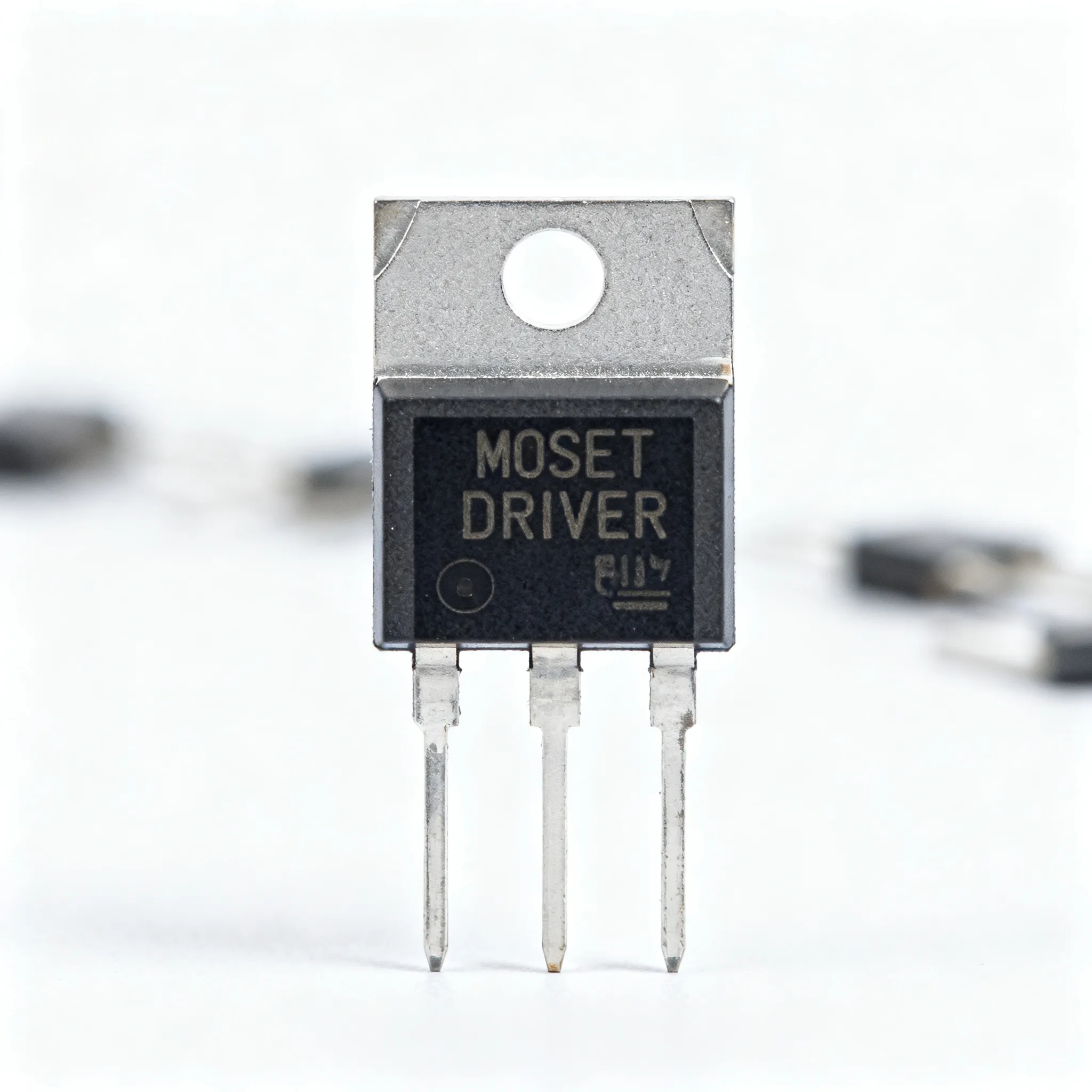
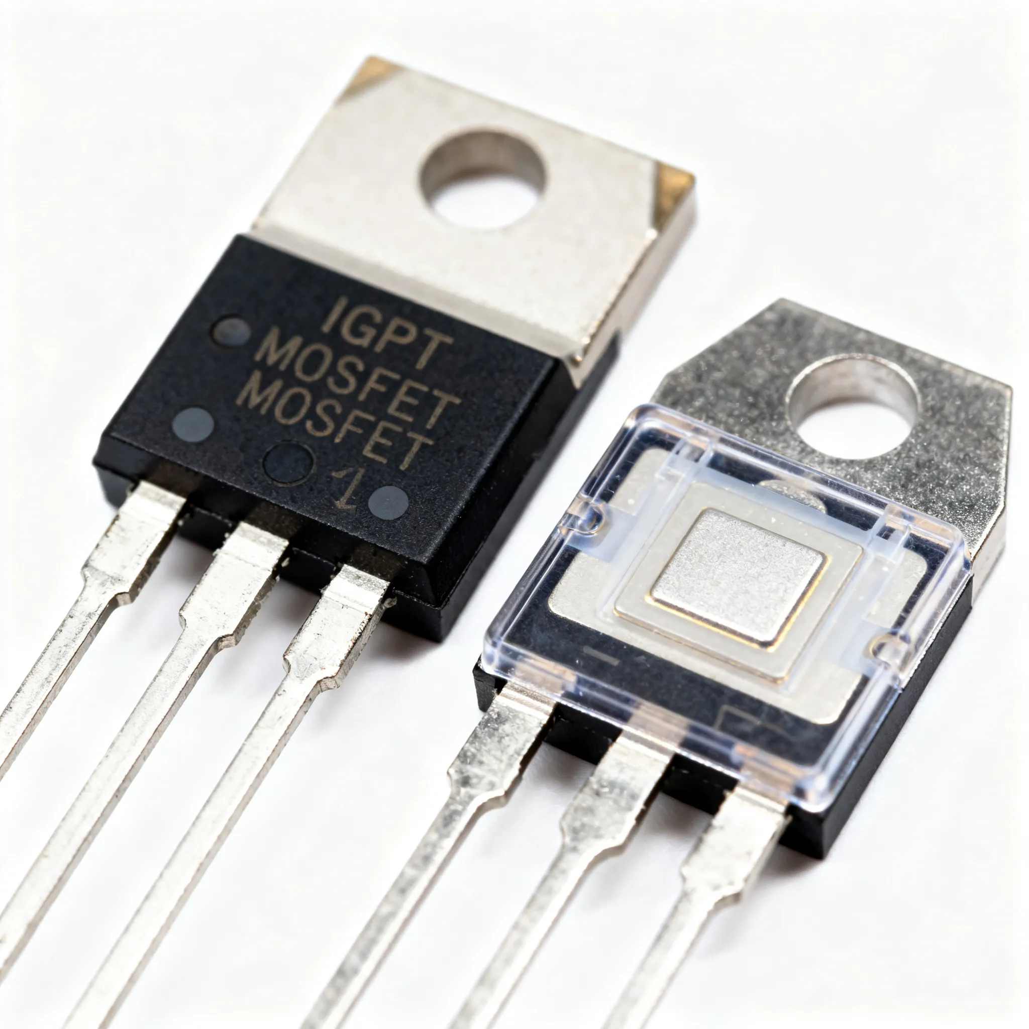
You improve system performance using nmos and digital logic architectures. These metal-oxide-semiconductor field-effect transistors rely on high electron mobility. Higher electron speed reduces switching resistance and dynamic power loss across every integrated circuit. A positive gate voltage creates an n-channel, driving current fast. Modern nmos design cuts thermal output while increasing total transistor density for 2026 systems. Evaluating nmos vs pmos trade-offs helps you choose the right transistor layout for high-frequency logic gate applications. Nova Technology Company (HK) Limited, a HiSilicon-designated solutions partner, delivers advanced semiconductor chip-level designs. By tuning each nmos transistor, you achieve lower threshold voltages and maximize raw power efficiency across smart devices.
Key Takeaways
- NMOS transistors use fast electrons to boost computer processing speeds.
- Higher electron mobility reduces energy loss and keeps chips cool.
- Engineers combine NMOS and PMOS switches to save battery life.
- Compact NMOS designs allow smaller and faster smart devices by 2026.
- Proper voltage control prevents chip overheating during heavy tasks.
Mechanics of the NMOS Transistor
How NMOS AND Gates Operate
You construct highly efficient logic circuits using nmos and digital gate configurations. To build an nmos and gate, semiconductor designers cascade an nmos transistor based NAND layout directly with a fast inverter. You arrange every nmos transistor in a strict series path leading straight to ground. This reliable topology effectively controls signal propagation across the semiconductor chip.
You link the source terminal of the initial nmos transistor directly to ground. Applying a positive gate voltage activates each switch along the series path. The logic high gate voltage turns on every nmos transistor simultaneously. This continuous activation connects the output terminal to ground and establishes standard logic behavior for digital processing.
Channel Formation and Electron Carrier Dynamics
Applying a positive gate voltage induces an electron-rich conducting channel in the silicon structure. This channel forms immediately beneath the thin oxide layer inside the n-channel mosfet transistor. The positive gate voltage generates a strong electric field across the semiconductor substrate. This field physically draws free electrons toward the oxide interface to enable conduction.
Electrons act as majority carriers inside each nmos transistor. In silicon devices, electron mobility operates 2 to 3 times faster than hole mobility in PMOS designs. Higher mobility significantly reduces on-state resistance during active operation. This movement enhances system switching characteristics while limiting dynamic energy loss in semiconductor design.
Threshold Voltage and Signal Integrity
Correctly biasing nmos circuits requires precise voltage management at all times. You must apply a continuous gate voltage above the internal transistor threshold level to maintain active current flow. Exceeding this threshold gate voltage expands the conducting channel thickness. Proper transistor gate voltage control permits continuous current flow from source to drain terminals.
Stable gate voltage drive maintains strong signal integrity across complex nmos logic paths. Adequate channel conductivity prevents signal distortion in fast switching operations. You optimize overall semiconductor behavior by managing transistor physical characteristics carefully. Transistor architecture delivers high operational speed across the semiconductor industry.
NMOS vs PMOS Efficiency
Key Behavioral Differences in Logic Design
You analyze nmos vs pmos characteristics to optimize modern digital circuits. An nmos transistor uses negative charge carriers called electrons. A PMOS transistor relies on positive holes for current flow. This fundamental difference shapes nmos vs pmos switching behavior across integrated circuits. Higher electron mobility gives each nmos logic switch faster response times and superior performance.
| Architecture Feature | NMOS | PMOS |
|---|---|---|
| Majority Charge Carrier | Electrons | Holes |
| Carrier Mobility | Higher | Lower |
| Relative Switching Speed | Faster | Slower |
| High-Speed Application Suitability | Highly Suitable | Less Favorable (Longer Delays) |
Lower switching resistance in nmos path configurations cuts dynamic energy loss. The nmos vs pmos operational differences directly impact overall dynamic power consumption. Fast electron movement reduces delay inside each transistor channel. Consequently, nmos designs achieve optimal throughput in high-speed semiconductor applications.
When to Choose Between NMOS and PMOS Logic
You choose between nmos and pmos logic layouts based on specific speed requirements. High-frequency applications demand rapid gate voltage transitions. Applying a positive gate voltage turns on the nmos gate instantly. You select nmos transistor switches to accelerate critical pull-down networks. Continuous gate voltage drive maintains stable gate propagation across every gate layout.
You choose between nmos and pmos configurations to minimize total silicon area. Compact nmos circuitry reduces physical footprint on the semiconductor chip. Reduced area requirements improve semiconductor manufacturing yield in modern semiconductor design. Stable gate voltage levels prevent unwanted current leakage during standby modes.
You balance nmos vs pmos elements inside standard CMOS logic gate circuits. Combining both transistor types eliminates steady-state power dissipation. Proper gate drive control ensures excellent signal integrity under high transistor density. Examining nmos vs pmos switching speeds helps you refine transistor threshold controls. Optimizing nmos vs pmos layouts improves overall transistor speed. Evaluating nmos vs pmos characteristics ensures low thermal output in fast processing units. Modern semiconductor systems rely on nmos and digital logic networks for maximum operational speed.
2026 Efficiency Gains in Digital Logic
Reduced Propagation Delay in Fast Switching
Modern high-speed circuits demand rapid signal transition times to maximize computing speed. You optimize these digital processing paths by leveraging higher electron carrier mobility in nmos logic layout. Electron motion across the conductive channel lowers internal switching resistance significantly. Consequently, logic switches change operational state without experiencing long propagation delays. You construct high-speed logic arrays by cascading these high-performance switches directly on the silicon die. Lower dynamic delay elevates overall system performance in high-frequency circuits.
Fast signal transition reduces active power dissipation across complex semiconductor chip topologies.
Applying a positive gate voltage establishes instantaneous electron conduction paths across each switch. Lower channel resistance accelerates capacitor charging cycles during fast switching operations. You refine overall transistor speed by balancing channel dimensions across high-frequency designs. Comparing nmos vs pmos propagation metrics reveals clear timing advantages for n-channel switches. Optimized switching characteristics accelerate total data processing throughput across dense transistor arrays. Strong transistor drive strength keeps digital signals crisp during high-frequency operation.
Thermal Management and Lower Parasitic Loss
Effective thermal control remains crucial for dense semiconductor layouts in 2026. Reducing dynamic power loss lowers baseline thermal dissipation across high-density digital architectures. Standard logic nodes suffer from excess parasitic capacitance during active cycles. Proper biasing nmos configurations minimizes unwanted charge accumulation along critical signal routes.
- You balance gate voltage drive strength to suppress localized hotspot formation across each transistor channel.
- You tune threshold transistor voltage levels to reduce steady-state leakage current paths.
- You optimize channel layout geometry to streamline chip-level power delivery.
Precise gate voltage alignment maintains consistent electrical performance without causing internal overheating. Lower thermal output protects delicate transistor junction boundaries from accelerated heat stress. Dynamic gate voltage management maintains system reliability across intensive processing workloads. Understanding key nmos vs pmos operational characteristics helps you layout efficient power distribution networks. Decreasing localized heat generation preserves structural integrity across the entire semiconductor substrate. Proper thermal management allows higher transistor density in modern integrated platforms. Effective semiconductor cooling preserves long-term circuit functionality under demanding dynamic thermal environments.
Microcontroller and IoT Circuit Integration
Smart hardware systems rely on compact logic blocks for low-power edge computing applications. You integrate nmos and PMOS components to create energy-efficient microcontroller architecture. Efficient nmos design reduces chip footprint while extending operational battery life in remote IoT applications. Nova Technology Company (HK) Limited serves as an authorized HiSilicon-designated solutions partner. They deliver advanced chip-level designs, IC system integration, and specialized microcontroller hardware tailored for modern IoT applications.
Compact logic integration enables fast signal routing inside small sensor modules. Proper gate voltage control prevents signal dropouts in battery-powered embedded hardware applications. Operating an nmos transistor switch reduces dynamic switching energy in modern IoT sensor applications. Optimizing each nmos transistor layout enhances overall gate switching performance under limited power budgets. Using nmos and digital logic gates enhances operational speed across industrial control applications. Selecting nmos and CMOS integrated options keeps power consumption minimal during continuous operation. Advanced semiconductor manufacturing techniques combine n-channel and p-channel features into compact integrated systems. System designers rely on these low-power topologies to extend field device operation. Integrated circuitry delivers steady processing efficiency across distributed network nodes.
You maximize performance by choosing nmos and logic designs. High electron mobility gives every nmos transistor fast switching speeds. Applying positive gate voltage opens the nmos channel quickly. You control key gate parameters to cut power loss in high-speed applications. Comparing nmos vs pmos layouts helps you select the best gate configuration.
Understanding nmos behavior allows engineers to balance dynamic efficiency across hardware by 2026. Optimized nmos path layouts reduce heat generation inside each semiconductor die. Low dynamic resistance keeps each transistor cool during active operation. Choosing nmos gate logic advances efficiency across processing applications. Evaluating nmos vs pmos tradeoffs streamlines next-generation semiconductor system architecture. Modern nmos designs drive efficient digital computation.
FAQ
Why does an nmos gate operate faster than a pmos gate?
An nmos gate uses negative electrons as primary carriers. Higher electron mobility reduces channel switching resistance inside each transistor switch. Faster conduction speeds up dynamic logic state transitions. This speed advantage makes n-channel design ideal for high-frequency semiconductor applications.
How do you control a logic switch in digital designs?
You apply a positive voltage to the nmos gate terminal. Exceeding the internal gate threshold creates a conductive channel inside the transistor. Current then flows from source to drain. Lowering the gate control signal turns off the switch to block active flow across the circuit path.
What key factors determine circuit selection for modern chips?
Evaluating nmos vs pmos trade-offs depends on carrier speed and physical area. An nmos transistor switch provides lower resistance in compact silicon layouts. Combining both types into CMOS gate networks prevents continuous current draw. This balance lowers power loss in complex semiconductor computing applications.
How does an nmos and gate reduce dynamic energy loss?
Cascading an nmos and circuit structure lowers propagation delay across signal networks. High carrier velocity reduces heat output during rapid gate state changes. Efficient nmos channel design reduces internal capacitance. You improve system efficiency by keeping each transistor gate driving energy low.
Why is n-channel logic evaluation vital for modern chip design?
Comparing nmos vs pmos parameters helps you balance overall processing throughput against total leakage current. Optimizing each nmos transistor channel size preserves signal integrity under high density. You achieve optimal power efficiency by adjusting transistor layout geometry around every gate on the chip.